Creating different width lines and spaces in a metal layer
- Summary
- Abstract
- Description
- Claims
- Application Information
AI Technical Summary
Benefits of technology
Problems solved by technology
Method used
Image

Examples
Embodiment Construction
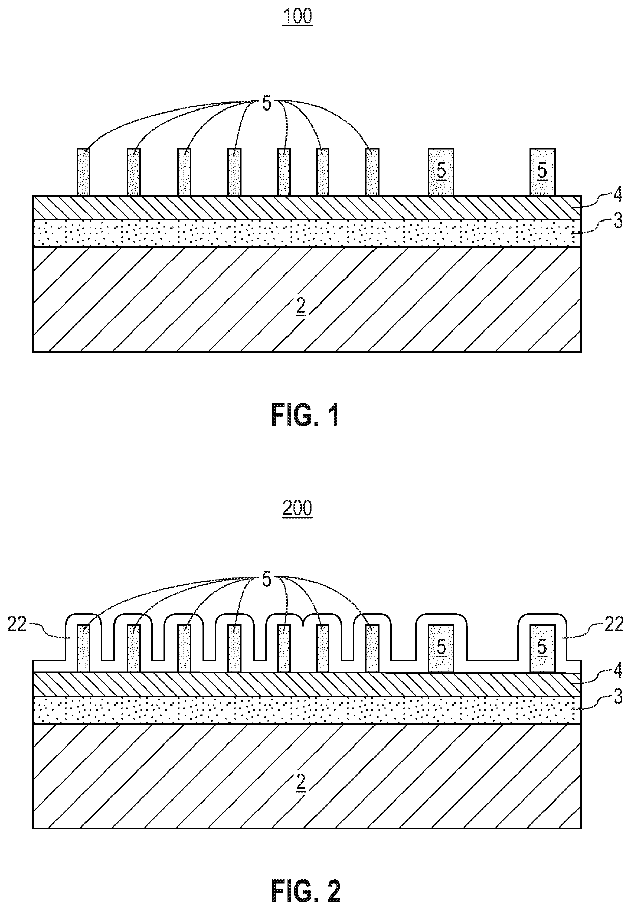
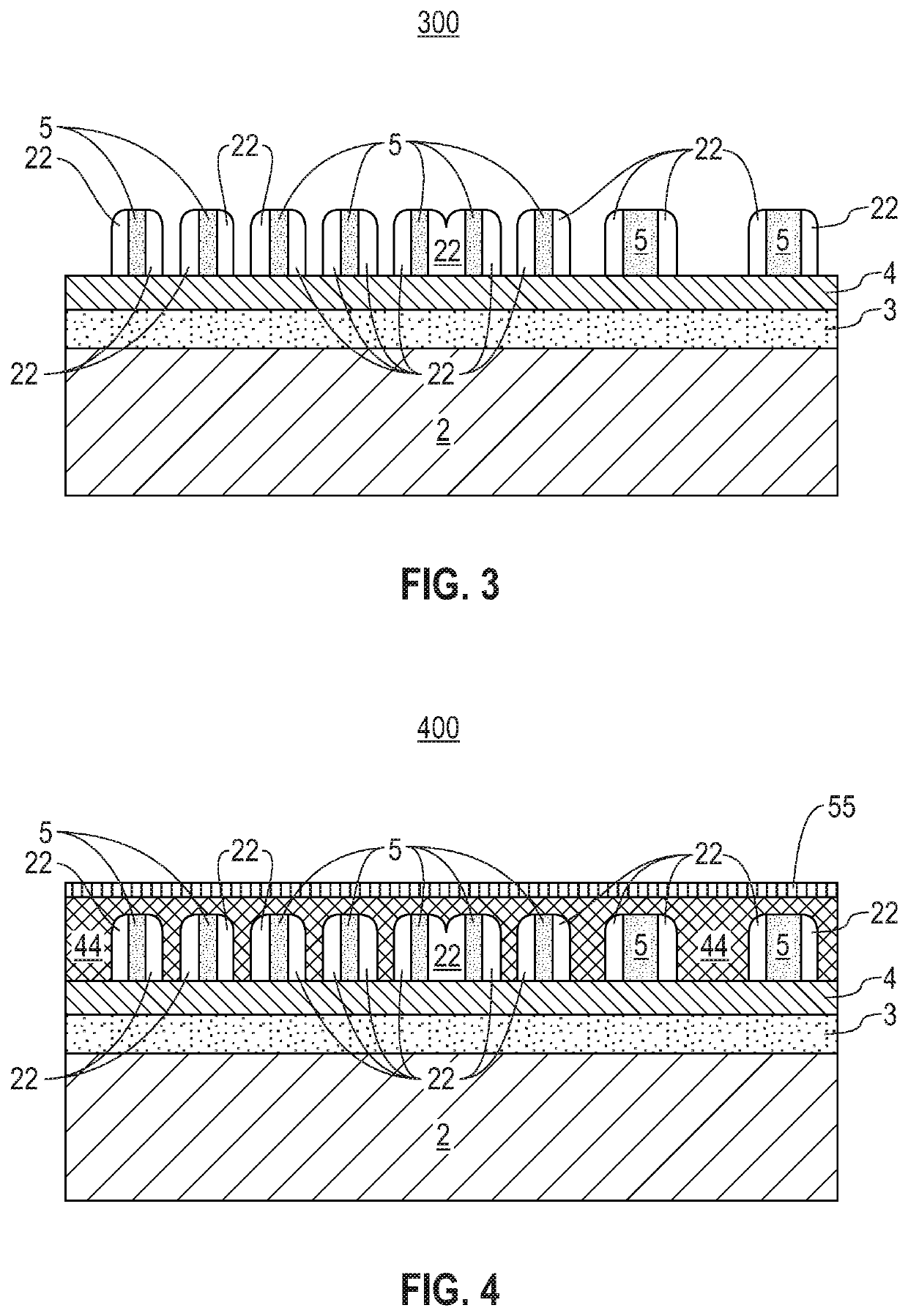
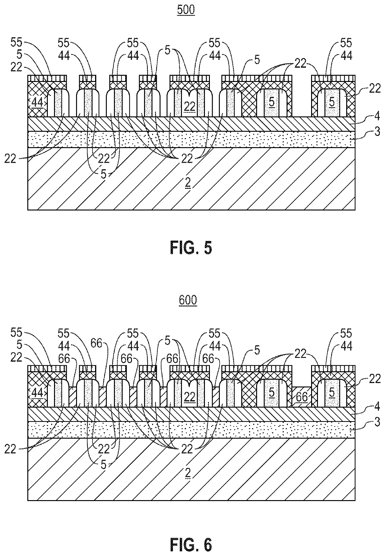
[0015]Embodiments of the present invention recognize that there is a need for increasing circuit density and increasing electrical performance in semiconductor devices. Embodiments of the present invention recognize that in order to increase circuit density there is a continual need for a reduction in line width and a reduction in the space between adjacent lines. Embodiments of the present invention recognize that to achieve electrical performance objectives, it is desirable to provide wider lines and wider spaces for some circuits. Embodiments of the present invention recognize that a method of providing both narrow lines with close spacing and wider lines with increased spacing between adjacent lines in the same metal layer of a semiconductor device is desirable to provide increased circuit density and improved electrical performance. Embodiments of the present invention recognize that providing semiconductor chip designers with design flexibility that allows the use of both fine...
PUM
 Abstract
Description
Claims
Application Information