Semiconductor package and method of manufacturing the semiconductor package

Active Publication Date: 2022-04-28
SAMSUNG ELECTRONICS CO LTD
View PDF2 Cites 0 Cited by
  • Summary
  • Abstract
  • Description
  • Claims
  • Application Information

AI Technical Summary

Benefits of technology

[0011]Accordingly, because the via pattern is located eccentric from the center of the pad pattern and the via pattern has a relatively small diameter, a flux gas generated from the conductive paste such as a solder paste may move to an e

Problems solved by technology

However, during a reflow process for mounting the capacitor, a flux gas vaporized from the solder paste m

Method used


Image

  • Semiconductor package and method of manufacturing the semiconductor package
  • Semiconductor package and method of manufacturing the semiconductor package
  • Semiconductor package and method of manufacturing the semiconductor package

Examples


Example

[0025]Hereinafter, some example embodiments will be explained in detail with reference to the accompanying drawings.

[0026]When the terms “about” or “substantially” are used in this specification in connection with a numerical value, it is intended that the associated numerical value includes a manufacturing tolerance (e.g., ±10%) around the stated numerical value. Moreover, when the words “generally” and “substantially” are used in connection with geometric shapes, it is intended that precision of the geometric shape is not required but that latitude for the shape is within the scope of the disclosure. Further, regardless of whether numerical values or shapes are modified as “about” or “substantially,” it will be understood that these values and shapes should be construed as including a manufacturing or operational tolerance (e.g., ±10%) around the stated numerical values or shapes.

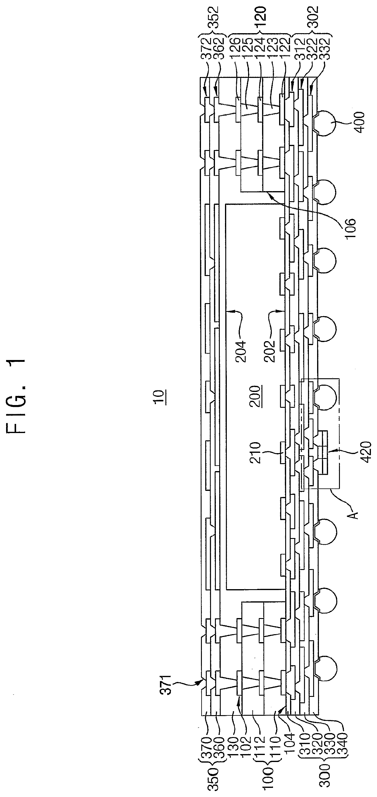
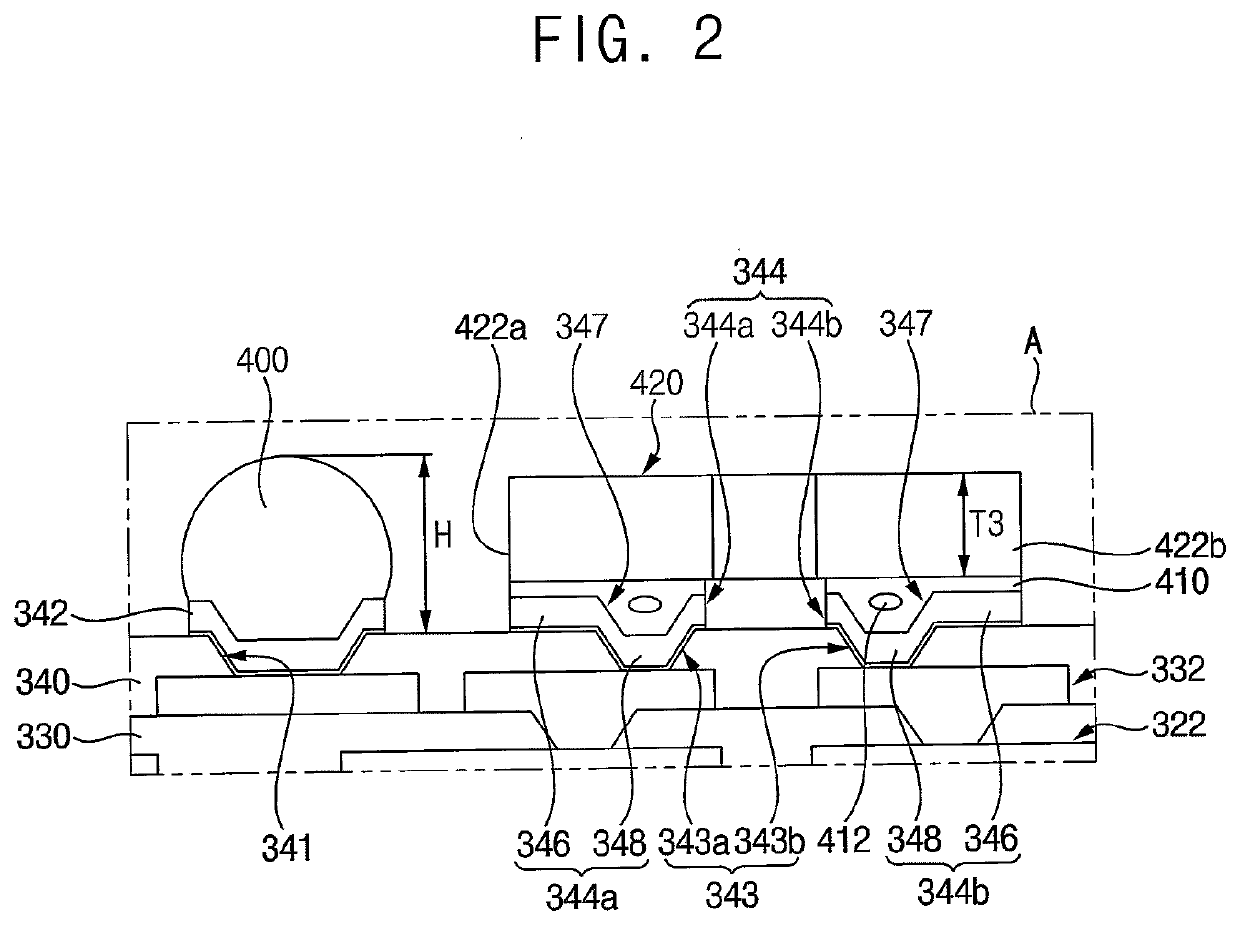
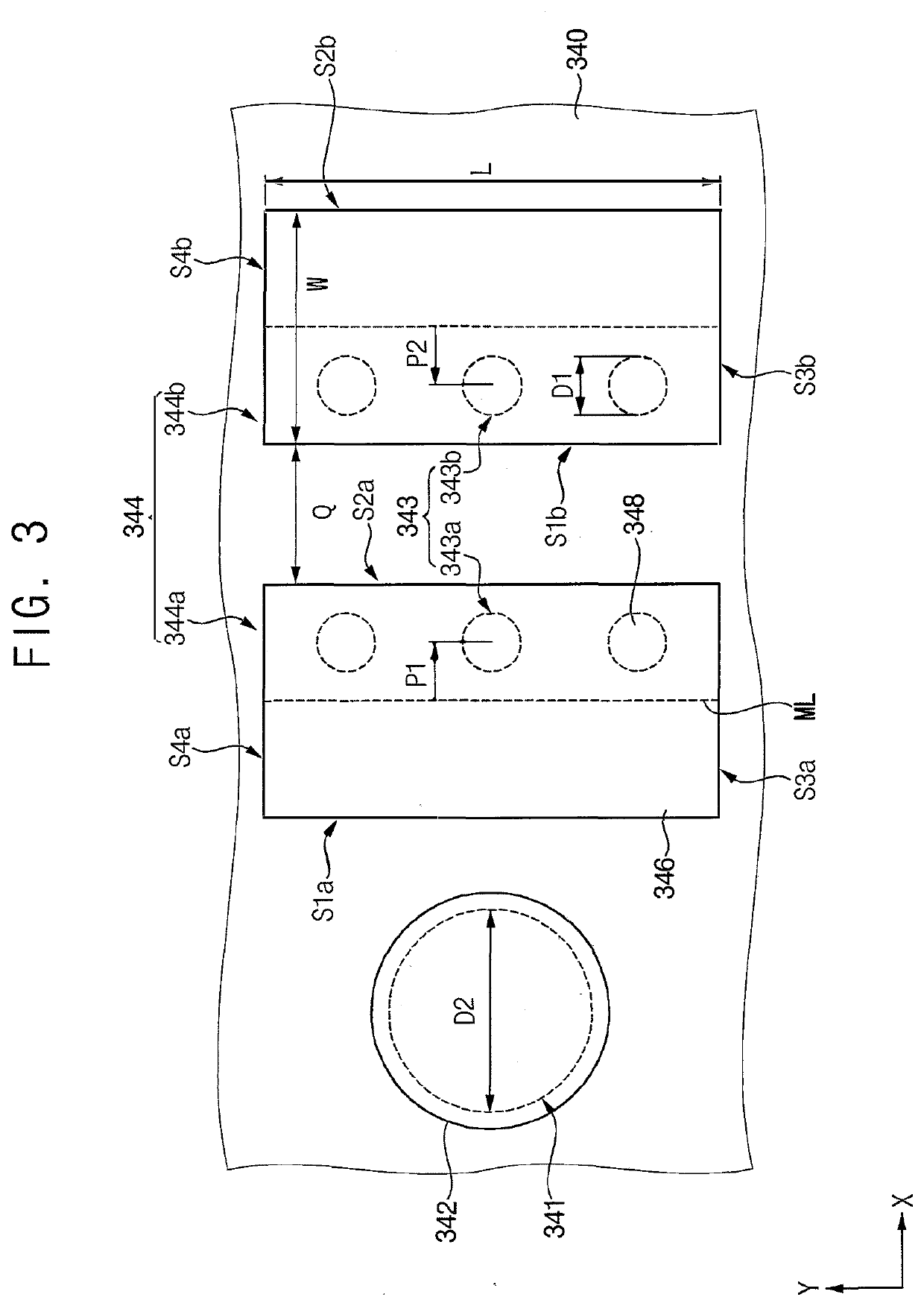
[0027]FIG. 1 is a cross-sectional view illustrating a semiconductor package in accordance with some ex...


PUM


Abstract

A semiconductor package including a core substrate, a semiconductor chip in the core substrate and having chip pads, a redistribution wiring layer covering a lower surface of the core substrate and including redistribution wirings electrically connected to the chip pads and a pair of capacitor pads exposed from an outer surface of the redistribution wiring layer, conductive pastes on the capacitor pads, respectively, and a capacitor via the conductive pastes and having first and second outer electrodes on the capacitor pads, respectively, may be provided. Each of the capacitor pads includes a pad pattern exposed from the outer surface of the redistribution wiring layer, and at least one via pattern at a lower portion of the pad pattern and electrically connected to at least one of the redistribution wirings. The via pattern is eccentric by a distance from a center line of the pad pattern.

Description

PRIORITY STATEMENT[0001]This application claims priority under 35 U.S.C. § 119 to Korean Patent Application No. 10-2020-0140455, filed on Oct. 27, 2020 in the Korean Intellectual Property Office (KIPO), the contents of which are herein incorporated by reference in their entirety.BACKGROUND1. Field[0002]Example embodiments relate to semiconductor packages and / or methods of manufacturing the semiconductor package. More particularly, example embodiments relate to semiconductor packages having a passive device and / or methods of manufacturing the same.2. Description of the Related Art[0003]A fan out package having a relatively thin thickness may include a thin film capacitor capable of implementing a thinner thickness as a passive device. The thin film capacitor may be a decoupling capacitor for an application processor and may be manufactured in the form of a Land-Side Capacitor (LSC). The LSC type capacitor may be mounted via a solder paste. However, during a reflow process for mountin...

Claims


Application Information

Patent Timeline
IPC IPC(8): H01L23/00
CPCH01L24/20H01L25/16H01L24/13H01L24/25H01L24/24H01L24/19H01L2224/73217H01L2224/24265H01L2224/24155H01L2224/25171H01L2224/2518H01L2224/13024H01L2224/13005H01L2224/2201H01L2224/2205H01L2224/2105H01L24/73H01L23/49822H01L23/49827H01L23/49838H01L23/49816H01L25/0657H01L2225/0651H01L2225/06568H01L25/105H01L2225/1058H01L25/50H01L23/642H01L2224/73265H01L2924/181H01L2924/15311H01L2224/48091H01L2224/32145H01L2224/32225H01L2224/48227H01L2225/1035H01L2225/1041H01L2225/1094H01L24/48H01L24/32H01L2224/04105H01L2224/12105H01L2924/00012H01L2924/00014H01L23/481H01L23/525H01L23/528H01L23/49513H01L24/11H01L24/06H01L24/09H01L2224/02379H01L2924/1443H01L2924/19041H01L2924/19104H01L2924/1431H01L2924/1436H01L2924/1437H01L2924/1441
Inventor JUNG, GYOYOUNGKIM, JINSUYANG, HYUNSUKLEE, KIJUJO, HOYEONJIN, IKKYU
Owner SAMSUNG ELECTRONICS CO LTD
Why Eureka
Try Eureka