Back Emission Display

Pending Publication Date: 2022-05-12
ELUX INC
View PDF10 Cites 5 Cited by
  • Summary
  • Abstract
  • Description
  • Claims
  • Application Information

AI Technical Summary

Benefits of technology

The patent describes a microLED display structure that can be manufactured by fluidic assembly, which simplifies the process of fabrication. The structure allows for microLED displays or tiles to be fabricated with processing and interconnection only on one side of the backplane. The display includes reflectors to direct the emitted light towards the viewer. The patent also describes a back emission microLED and a power interface layer with control circuits for the microLED. The technical effects of this patent include simplifying the manufacturing process of microLED displays and improving the efficiency of the display.

Problems solved by technology

As a consequence, the efficiency of an LCD display may be less than 4% and the contrast ratio is limited by light leaking through the cell.
OLED displays are direct emitting so the contrast ratio is high, but the organic materials can be subject to long-term degradation causing image burn-in.
MicroLEDs are fabricated from metalorganic chemical vapor deposition (MOCVD) wafers like those used to make LEDs for general lighting, which makes the cost per device very low but also introduces issues unique to microLED technology.
Both the methods of FIGS. 2 and 3 are complex with processing on both sides of the backplane, so integration of the 2-sided interconnect scheme with the TFT fabrication and microLED assembly is quite difficult.
In addition, the laser cut vias are formed one at a time, so the cost becomes prohibitive for consumer displays requiring millions of vias.
The undesirable result is that light from one pixel can emerge from an adjacent pixel, effectively contaminating the image of the adjacent pixel.

Method used


Image

  • Back Emission Display
  • Back Emission Display
  • Back Emission Display

Examples


Embodiment Construction

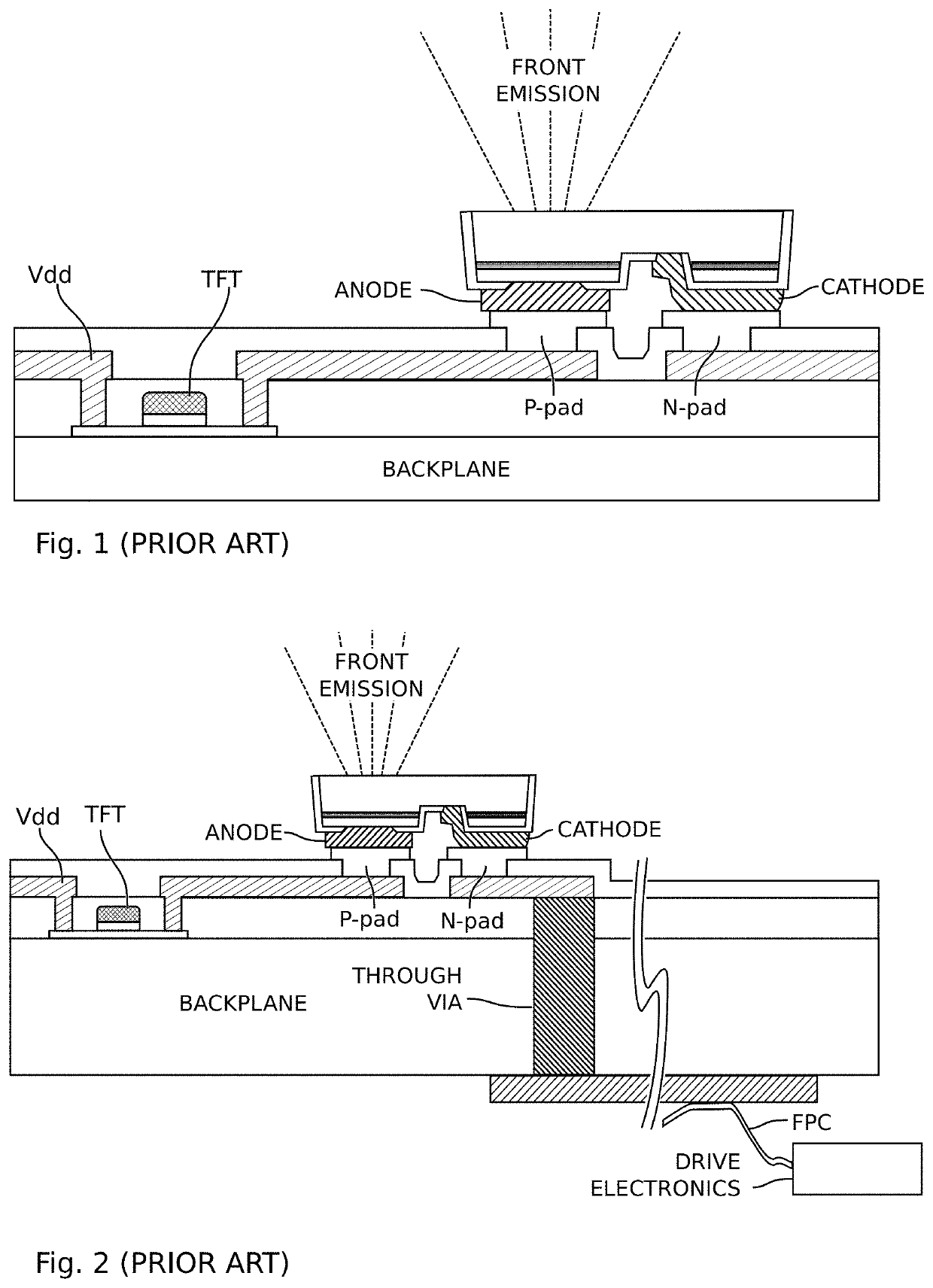
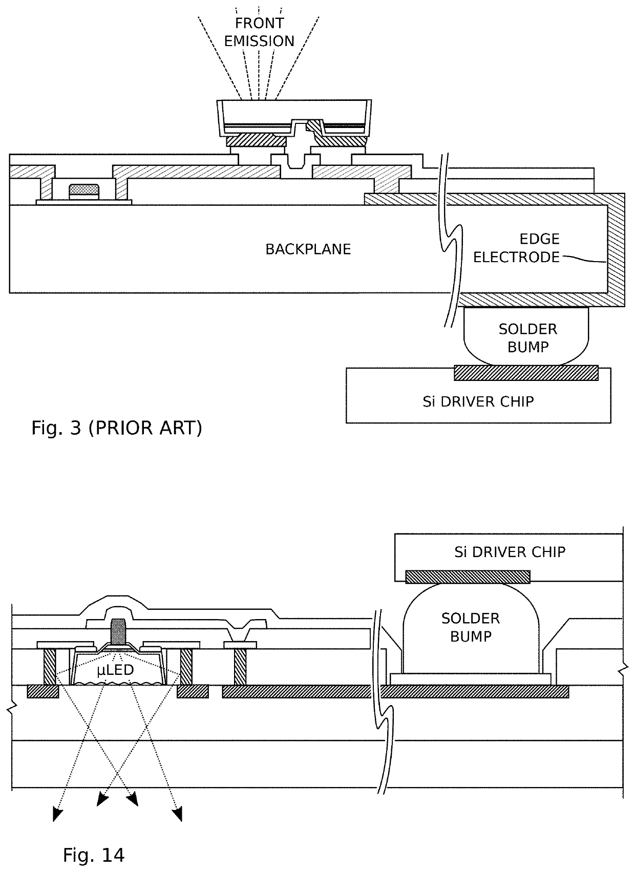
[0035]The general process for making a microLED display using inorganic LEDs and fluidic assembly on a display backplane has been reported in U.S. Pat. No. 9,825,202, entitled DISPLAY WITH SURFACE MOUNT EMISSIVE ELEMENTS and U.S. Pat. No. 10,418,527, entitled SYSTEM AND METHOD FOR THE FLUIDIC ASSEMBLY OF EMISSIVE DISPLAYS, incorporated herein by reference. The geometric requirements for fluidic assembly are presented in U.S. Pat. No. 9,825,202 starting at Col. 12, ln. 56, and shown in FIG. 16. In particular, the process flow for making a suitable display backplane is described starting at Col. 13, ln. 26, and shown in FIG. 17. The electrical requirements are described in Ser. No. 16 / 727,186, entitled SYSTEM AND METHOD FOR LIGHT EMITTING DIODE (LED) DISPLAY REPAIR, which is incorporated herein by reference. The display substrate described herein uses the same row and column arrangement of TFT control circuits as previously described, but the display architecture has been inverted so ...


PUM


Abstract

Disclosed herein is a micro light emitting diode (microLED) display structure with emission from the back side of a transparent substrate, which can be manufactured by fluidic assembly. The architecture allows microLED displays or display tiles to be fabricated simply, with processing and interconnection only on one side of the backplane. The structure may incorporate reflectors in the fluidic assembly structures to direct substantially all of the emitted light toward the viewer. Also disclosed are microLEDs and emission backplanes designed to support a back emission display.

Description

RELATED APPLICATIONS[0001]Any and all applications, if any, for which a foreign or domestic priority claim is identified in the Application Data Sheet of the present application are hereby incorporated by reference under 37 CFR 1.57.BACKGROUND OF THE INVENTION1. Field of the Invention[0002]This invention generally relates to emissive displays and, more particularly, to a back emission display and well as supporting light emitting diodes (LEDs) and back emission backplanes.2. Description of the Related Art[0003]A red-green-blue (RGB) display is composed of pixels that emit light at three wavelengths corresponding to the visible colors red, green, and blue. The RGB components of the pixel, each of which is referred to as a sub-pixel, are energized in a systematic way to additively produce the colors of the visible spectrum. There are several display types that produce the RGB images in different ways. Liquid crystal displays (LCD) are the most prevalent technology, and they produce RG...

Claims


Application Information

Patent Timeline
IPC IPC(8): H01L33/60H01L25/16H01L27/12H01L33/24H01L25/075
CPCH01L33/60H01L25/167H01L27/124H01L33/0093H01L25/0753H01L27/127H01L33/24H01L21/67144H01L21/7806H01L24/00H01L33/0095H01L33/62H01L2933/0066H01L33/20H01L33/38H01L2933/0016H01L2933/0058H01L2224/16225H01L33/486H01L2933/0033
Inventor SCHUELE, PAUL J.ULMER, KURTSASAKI, KENJILEE, JONG-JAN
Owner ELUX INC
Why Eureka
Try Eureka