Radiation imaging apparatus and manufacturing method of same

a technology of radiation imaging apparatus and manufacturing method, which is applied in the direction of x/gamma/cosmic radiation measurement, radioation controlled devices, instruments, etc., can solve the problems of matrix panel operation failure, readout failure, described failure, etc., and achieve the effect of reducing the short circui

Pending Publication Date: 2022-06-16
CANON KK
View PDF0 Cites 0 Cited by
  • Summary
  • Abstract
  • Description
  • Claims
  • Application Information

AI Technical Summary

Benefits of technology

[0006]The present disclosure is directed to providing a manufacturing method that may reduce a short circuit between wiring lines of an FPC due to soot in a radiation imaging apparatus using a flexible matrix panel, and a radiation imaging apparatus that is less likely to cause a short circuit between wiring lines of an FPC due to soot.

Problems solved by technology

This results in a connection failure with the drive circuit and causes an operation failure of the matrix panel.
Furthermore, this results in a connection failure with the readout circuit and causes a readout failure, i.e., a failure to read out a signal from the matrix panel.
There are various methods for removing (cleaning) soot, but cleaning may, on the contrary, spread the soot and have a risk of causing the above-described failure.

Method used


Image

  • Radiation imaging apparatus and manufacturing method of same
  • Radiation imaging apparatus and manufacturing method of same
  • Radiation imaging apparatus and manufacturing method of same

Examples


Embodiment Construction

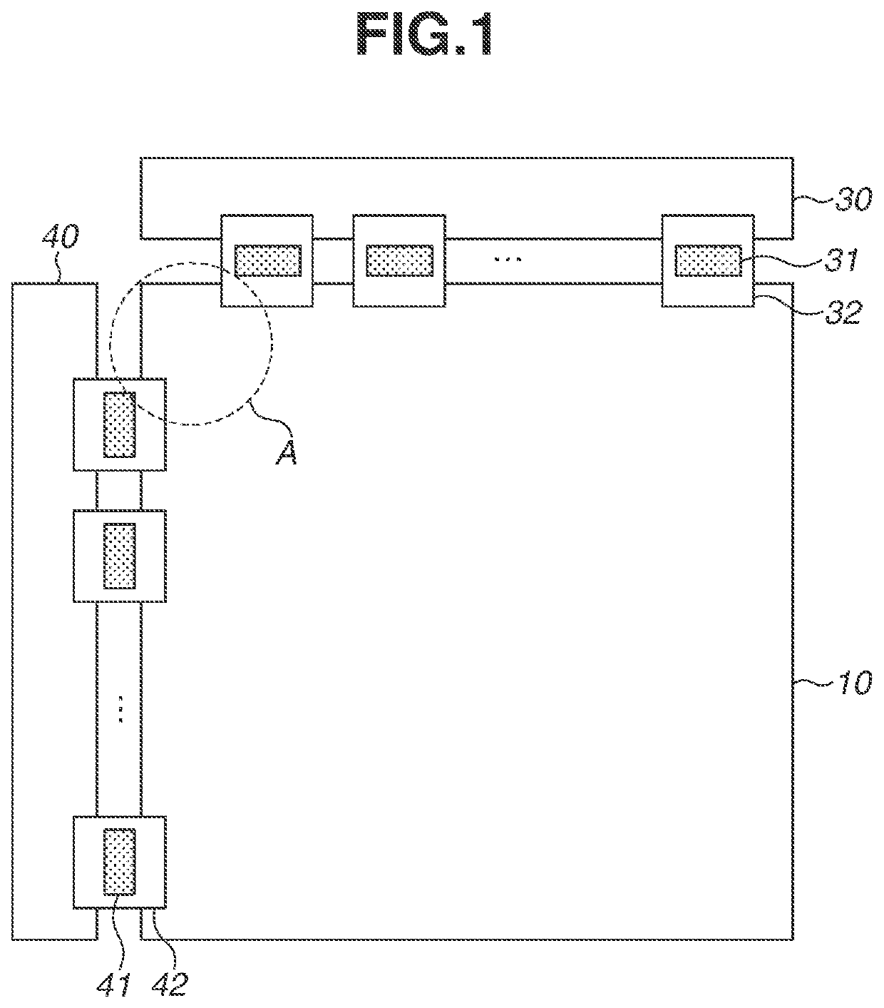
[0022]FIG. 1 is a plan view illustrating a state where an integrated circuit is coupled to a flexible radiation detection panel according to a first exemplary embodiment.

[0023]Two types of integrated circuits (a readout circuit 31 and a drive circuit 41) mounted on a circuit substrate are coupled to a radiation detection panel 10. The readout circuit 31 is a circuit configured to read out electrical signals from a plurality of pixels 15 provided on a matrix panel 11 included in the radiation detection panel 10. The readout circuit 31 is coupled to a readout device 30 via a readout wiring member 32. The drive circuit 41 is a circuit configured to supply drive signals to the plurality of pixels 15. The drive circuit 41 is coupled to a drive device 40 via a driving wiring member 42.

[0024]According to the present exemplary embodiment, these two types of wiring members, i.e., the readout wiring member 32 and the driving wiring member 42, include flexible printed boards (FPCs). These wiri...


PUM

PropertyMeasurementUnit
flexibleaaaaaaaaaa
conductiveaaaaaaaaaa
electricalaaaaaaaaaa

Abstract

A method of manufacturing a radiation imaging apparatus includes electrically connecting a first surface of a flexible insulating layer to a conductive portion of a circuit substrate, covering an exposed portion of the conductive portion with a protection layer, and separating the flexible insulating layer from a substrate in contact with a second surface of the flexible insulating layer. The circuit substrate includes an integrated circuit mounted on the circuit substrate. The flexible insulating layer includes, on the first surface, a plurality of pixels arranged in a two-dimensional matrix to convert radiation into an electrical signal. The second surface of the flexible insulating layer is opposite to the first surface of the flexible insulating layer. The flexible insulating layer is separated from the substrate by irradiating the second surface with light transmitting through the substrate.

Description

BACKGROUNDField[0001]The present disclosure relates to a radiation imaging apparatus and a method of manufacturing a radiation imaging apparatus.Description of the Related Art[0002]A manufacturing technique for display devices using thin-film transistors (TFTs) has been applied to matrix panels for large-area sensors including TFTs and semiconductor photoelectric conversion elements. A matrix panel is used as a radiation detection apparatus in combination with a scintillator configured to convert radiation into light. A matrix panel is typically formed on a glass substrate; however, flexible matrix panels using a resin, and the like, have been developed to hold promise for a reduction in the weight of the apparatus as well as for the durability against impact and deformation, and the flexible matrix panels are also being used in radiation detection apparatuses.[0003]A typical method of forming a flexible matrix panel is to place a thin film of a flexible insulating layer made of a r...

Claims


Application Information

Patent Timeline
Patent Type & Authority Applications(United States)
IPC IPC(8): G01T1/20H01L27/146
CPCG01T1/20189G01T1/20184H01L27/1469H01L27/14661H01L27/14663H01L27/14603H01L27/14612H01L27/14643H01L27/14683G01T1/20G01T1/202H01L27/14685
Inventor OFUJI, MASATOSASAKI, YOSHITOINOUE, MASATOISHII, TAKAMASA
Owner CANON KK
Why Eureka
Try Eureka