Semiconductor device having carbon nanotube interconnects contact deposited with different orientation and method for manufacturing the same

a carbon nanotube and interconnect technology, applied in the direction of semiconductor devices, semiconductor/solid-state device details, electrical apparatus, etc., can solve the problems of short circuits in the device structure, poor performance, and lag in the signal transmission speed of metal wirings, so as to improve the anti-electromigration ability, improve the thermal conductivity, and improve the effect of physical structur

Active Publication Date: 2013-04-02
INST OF MICROELECTRONICS CHINESE ACAD OF SCI
View PDF11 Cites 0 Cited by
  • Summary
  • Abstract
  • Description
  • Claims
  • Application Information

AI Technical Summary

Benefits of technology

[0008]In the embodiments of the present invention, the metal wiring and the interconnect structure with incorporated vias, which are formed according to the method for manufacturing a semiconductor structure, are formed with a conductive material and a nanotube / wire layer surrounded by the conductive material; since the nanotube / wire has unique physical structure and physical and chemical properties, it enables the conductive layer to have better thermal conductivity, conductivity and high anti-electromigration capability, thereby improving the signal transmission speed at the conductive layer, which thus enables its signal transmission speed to match with the increasingly enhanced speed of the devices. Besides, since the carbon nanotube / wire is a structure formed by single-layer carbon atoms or metal atoms, thus it is favorable for preventing the metal or other ions within the conductive material from diffusing into other places in the semiconductor structure, and is able to provide an interconnect structure of high quality, and also is able to reduce short circuits taking place in the semiconductor structure.

Problems solved by technology

However, the scaling in the sizes of metal wirings also results in increase of resistance of the metal wirings, which may consequently cause such a problem that the signal transmission speed of the metal wirings lags behind the operation speed of the devices.
Nonetheless, metal ions in these metal materials would easily diffuse into the semiconductor structure, and thus cause shorts in the device structure or other problems of poor performance.

Method used


Image

  • Semiconductor device having carbon nanotube interconnects contact deposited with different orientation and method for manufacturing the same
  • Semiconductor device having carbon nanotube interconnects contact deposited with different orientation and method for manufacturing the same
  • Semiconductor device having carbon nanotube interconnects contact deposited with different orientation and method for manufacturing the same

Examples


Embodiment Construction

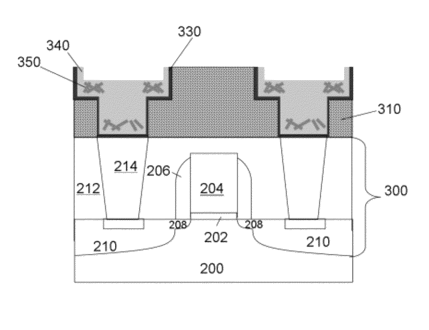
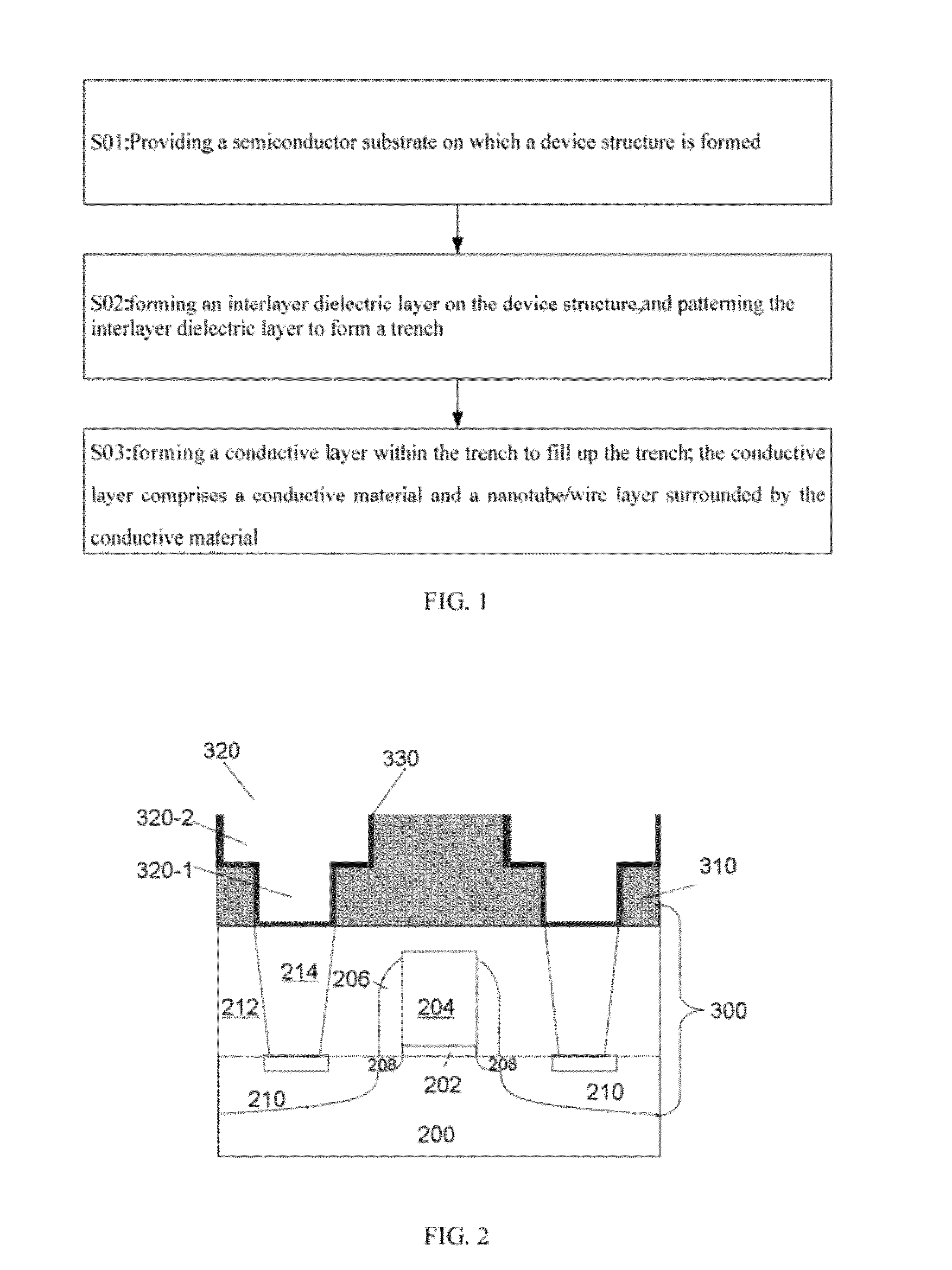
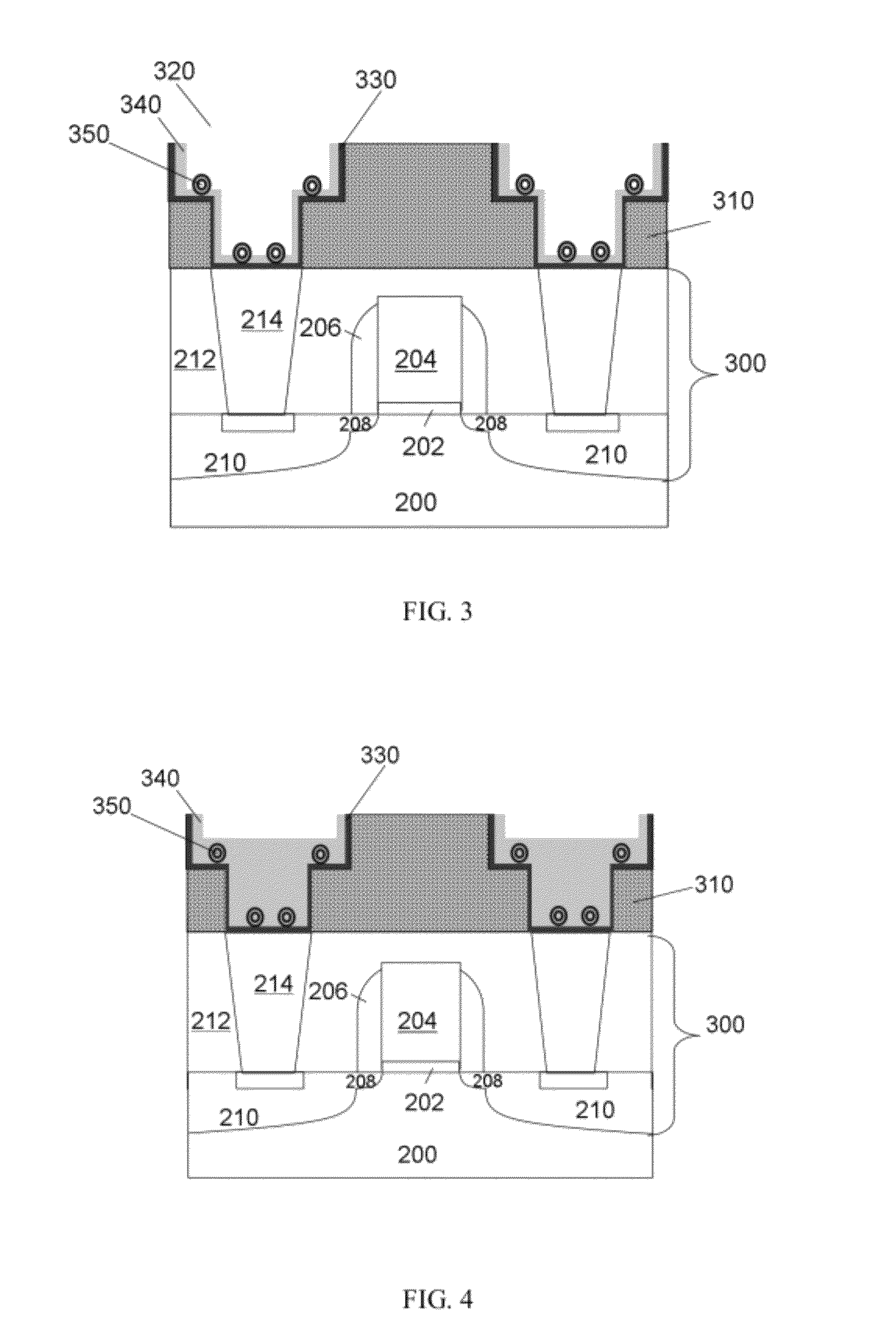
[0014]The present invention generally relates to a method for manufacturing a semiconductor structure. The following disclosure provides a plurality of different embodiments or examples to achieve different structures of the present invention. To simplify the disclosure of the present invention, description of components and arrangements of specific examples is given. Of course, they are only illustrative and not limiting the present invention. Moreover, in the present invention, reference number(s) and / or letter(s) may be repeated in different embodiments. Such repetition is for the purposes of simplification and clearness, and does not denote the relationship between the respective embodiments and / or arrangements being discussed. In addition, the present invention provides various examples for specific processes and materials. However, it is obvious for a person of ordinary skill in the art that other processes and / or materials may alternatively be utilized. Furthermore, the follo...


PUM


Abstract

The present invention relates to a semiconductor device structure and a method for manufacturing the same; the structure comprises: a semiconductor substrate on which a device structure is formed thereon; an interlayer dielectric layer formed on the device structure, wherein a trench is formed in the interlayer dielectric layer, the trench comprises an incorporated via trench and a conductive wiring trench, and the conductive wiring trench is positioned on the via trench; and a conductive layer filled in the trench, wherein the conductive layer is electrically connected with the device structure; wherein the conductive layer comprises a conductive material and a nanotube / wire layer surrounded by the conductive material. Wherein, the conductive layer comprises a conductive material and a nanotube / wire layer surrounded by the conductive material. The conductive layer of the structure has better thermal conductivity, conductivity and high anti-electromigration capability, thus is able to effectively prevent metal ions from diffusing outwards.

Description

CROSS REFERENCE TO RELATED APPLICATIONS[0001]This application is a national stage application, filed under 35 U.S.C. §371, of International Application No. PCT / CN2011 / 071345, filed Feb. 26, 2011, which claims the priority of Chinese Patent Application No. 201010264536.6, filed Aug. 26, 2010, all of which are hereby incorporated by reference in their entirety.FIELD OF THE INVENTION[0002]The present invention generally relates to a semiconductor device structure and a method for manufacturing the same, and specifically, to a semiconductor device structure with an interconnect structure of better performance and a method for manufacturing the same.BACKGROUND OF THE INVENTION[0003]With the rapid development of the semiconductor technology, integrated circuits with better performance and more powerful functions require greater element density, thus the sizes of CMOS (Complementary Metal Oxide Semiconductor) devices and of components such as metal wirings have to be further scaled, so as ...

Claims


Application Information

Patent Timeline
Patent Type & Authority Patents(United States)
IPC IPC(8): H01L29/40H01L21/00
CPCH01L21/76807H01L21/76843H01L21/76846H01L21/76847H01L21/76877H01L23/53276H01L2924/0002H01L2221/1094H01L2924/00
Inventor ZHONG, HUICAILIANG, QINGQINGLUO, ZHIJIONGZHU, HUILONG
Owner INST OF MICROELECTRONICS CHINESE ACAD OF SCI
Why Eureka
Try Eureka