Method for production of electronic circuit board

a technology of electronic circuit board and production method, which is applied in the direction of resistive material coating, printed circuit assembling, metallic material coating process, etc., can solve the problems of interfering the fine spacing of circuit boards, printing of solder pastes encountering difficulty in coping with fine pitch patterns, and difficulty in adding to the thickness of solder layers, etc., to achieve simple operation, reduce short circuits, and exalt the reliability of electronic circuit boards

Inactive Publication Date: 2011-10-18
SHOWA DENKO KK
View PDF19 Cites 0 Cited by
  • Summary
  • Abstract
  • Description
  • Claims
  • Application Information

AI Technical Summary

Benefits of technology

[0025]By the method contemplated by this invention for the production of an electronic circuit board, it has been made possible to form a fine solder circuit pattern with a simple operation. The method particularly has brought about an effect of decreasing the short circuits with a solder metal between the adjacent circuit patterns even in a very fine circuit pattern and has conspicuously exalted the reliability of an electronic circuit board. Further, by the method contemplated by this invention for the production of an electronic circuit board, it has been made possible to materialize miniaturization and exaltation of high reliability of a circuit board having electronic parts mounted thereon and provide an electronic device of outstanding characteristic properties.

Problems solved by technology

The method for producing a solder circuit by the plating technique, however, incurs difficulty in adding to the thickness of the solder layer, and the HAL method and the method resorting to the printing of a solder paste encounter difficulty in coping with the fine pitch pattern.
Since this method effects dry deposition of the solder powder on the circuit board, it entails such problems as suffering the powder to be electrostatically deposited on an extraneous portion, inducing drift of the powder, interfering the fine spacing of a circuit board and preventing the powder from being efficiently utilized.
These problems gain in conspicuousness particularly when the solder powder to be used has a very fine size.

Method used


Image

  • Method for production of electronic circuit board
  • Method for production of electronic circuit board
  • Method for production of electronic circuit board

Examples


example 1

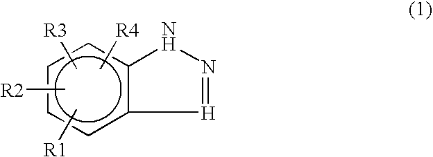
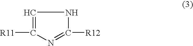
[0069]A printed-wiring board having the smallest electrode spacing of 50 μm was manufactured. As a stickiness imparting compound solution, an aqueous 2 mass % solution of an imidazole-based compound conforming to the general formula (3) by having a hydrogen atom for R11 and an alkyl group of C11H23 for R12 was used with the pH value thereof adjusted with acetic acid to about 4. This aqueous solution was heated to 40° C. and the aforementioned printed-wiring board pretreated with an aqueous hydrochloric acid solution was immersed in the heated aqueous solution, with the result that a sticky substance was formed on the surface of a copper circuit.

[0070]Subsequently, the printed-wiring board was immersed for 30 seconds in a solution that was obtained by causing a 96.5Sn-3.5Ag solder powder having an average particle diameter of about 20 μm to be dispersed in a concentration of 10 apparent volume % in water. Thereafter, the printed-wiring board was taken out of the solution, washed ligh...

examples 4 to 6

[0080]The experiments of forming a solder bump were made by following the procedure of Example 1 while using other conditions as shown in Table 3. The results are shown in Table 3.

[0081]

TABLE 3Rating ResultsTreatment ConditionsState ofWettingMethodCoating ofAddition ofsepositionproperty ofofSolderpowdertriethyl amineofsolder afterEx.depositioncompositionwith Snto waterpowderreflowingEx. 4In waterSn—8Zn—3BiNoNo◯ΔEx. 5In waterSn—8Zn—3BiNoYes◯◯Ex. 6In waterSn—8Zn—3BiYesNo◯◯Ex. 1In waterSn—3.5AgNoNo◯◯


PUM

PropertyMeasurementUnit
pHaaaaaaaaaa
frequencyaaaaaaaaaa
particle diameteraaaaaaaaaa

Abstract

A method for the deposition of a soldering powder to an electronic circuit board includes the steps of imparting stickiness to an exposed metal surface of a substrate and depositing a soldering powder to the resultant sticking part in a liquid body. The method can further include the steps of heating the substrate, thereby fusing the soldering powder, and forming a solder circuit.

Description

CROSS REFERENCE TO RELATED APPLICATIONS[0001]This application is an application filed under 35 U.S.C. §111 (a) claiming the benefit pursuant to 35 U.S.C. §119 (e) (1) of the filing dates of Provisional Application No. 60 / 572,946 filed May 21, 2004 and Japanese Patent Application No. 2004-139394 filed May 10, 2004 pursuant to 35 U.S.C. §111 (b).TECHNICAL FIELD[0002]This invention relates to a method for the production of an electronic circuit board. More particularly, the invention relates to a method for forming a solder layer on the surface of a fine conductive circuit electrode on an electronic circuit board, particularly a printed-wiring board.BACKGROUND ART[0003]In recent years, a printed-wiring board having a circuit pattern formed on an insulating substrate, such as a plastic substrate, a ceramic substrate or a metallic substrate coated with plastic, has been developed. Means to configure an electronic circuit by soldering electronic components, such as an IC element, a semico...

Claims


Application Information

Patent Timeline
Patent Type & Authority Patents(United States)
IPC IPC(8): B23K31/02H05K3/34
CPCH05K3/3484H05K2203/0292Y10T29/49144H05K2203/0485H05K2203/0425H05K3/3485H05K3/34
Inventor SAKAI, TAKEKAZUSHOJI, TAKASHI
Owner SHOWA DENKO KK
Why Eureka
Try Eureka