Transfer resin for transferring an LED chip, and an apparatus for transferring an LED chip by using the same

Pending Publication Date: 2022-08-11
LIGHTIZER KOREA
View PDF0 Cites 0 Cited by
  • Summary
  • Abstract
  • Description
  • Claims
  • Application Information

AI Technical Summary

Benefits of technology

The present invention relates to a display device with various pitches that can be manufactured using a micro-unit LED chip transfer method without errors. This method allows for the selective transfer of multiple chips on a base substrate using predetermined UV and heat. It also provides a method to increase manufacturing ease, lower manufacturing cost, and zero transfer errors of LED chips in micro units by using a photoactive agent as a transfer resin and eliminating errors in display panel fabrication due to peeling or detaching of the LED chip before transfer by having a clip-up structure.

Problems solved by technology

Therefore, a simple Pick & Place method takes at least a month to make a 40-inch display device.
However, since the size of the μ-LED chip manufactured on the sapphire substrate is small and thin, there occurs such problems as damage to the chip, failure to transfer the μ-LED chip one by one, failure to align the chip, or tilt of the chip, and so on, during the pick and place transfer process transferring the μ-LED chip one by one.
In addition, there is a problem that the transfer process takes too long.
Japanese Patent Application Publication No. 2019-015899 discloses a technique of expanding thermally expandable particles to weaken the adhesive force and exfoliating the same as a transfer method of chip parts, but there are problems such as uniform mixing of thermally expandable particles and technology of ensuring uniform adhesive force.

Method used


Image

  • Transfer resin for transferring an LED chip, and an apparatus for transferring an LED chip by using the same
  • Transfer resin for transferring an LED chip, and an apparatus for transferring an LED chip by using the same
  • Transfer resin for transferring an LED chip, and an apparatus for transferring an LED chip by using the same

Examples


Embodiment Construction

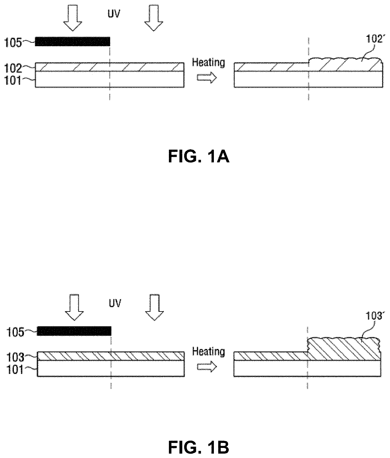
[0048]In the description of the embodiment, when described as being formed “upper (top) or lower (bottom)” of each element, two elements are directly in contact with each other or at least one other element is disposed between the two elements. In addition, when expressed as “up (up) or down (down)”, it may include not only upward but also downward meanings with respect to one element.

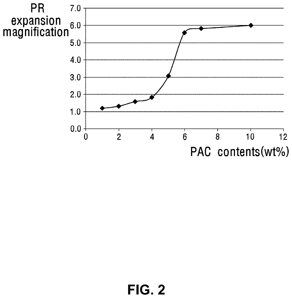
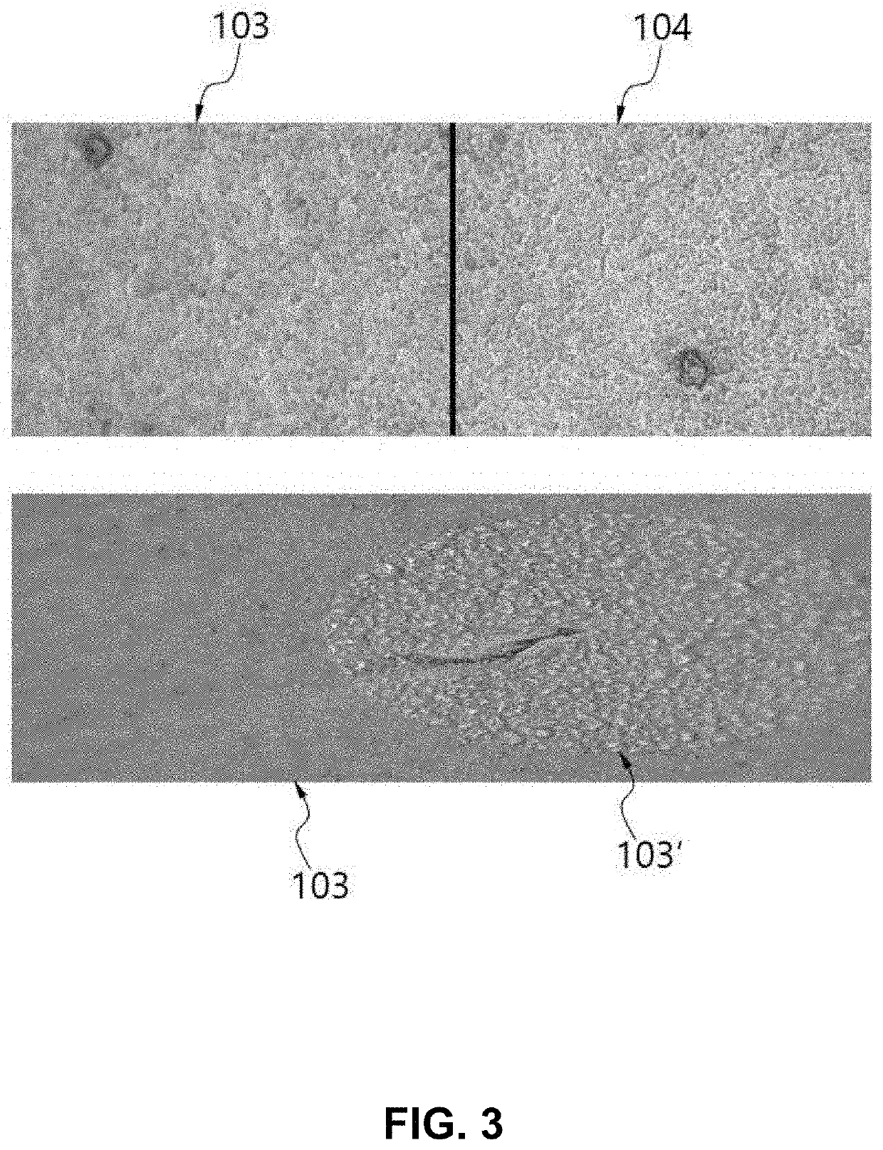
[0049]In the drawings, the thickness or size of each layer is exaggerated, omitted, or schematically illustrated for convenience and clarity of description. In addition, the size of each element does not fully reflect the actual size.

[0050]Chip, CSP, LED pixel CSP, and LED subpixel CSP used in the present invention may be defined as follows.

[0051]A chip is a concept that includes all of an LED chip, an RGB chip, an R chip, a G chip, a B chip, a mini LED chip, and a micro LED chip. Hereinafter, for convenience of description, the chip is described as an R chip, a G chip, or a B chip, but it should be no...


PUM


Abstract

The present invention relates to a transfer technology using a technique of transferring LED chips formed on a wafer to another carrier substrate and display panel, a transfer resin, and an apparatus for transferring an LED chip and a display panel using a resin which expands when light is applied. An apparatus for transferring an LED chip in accordance with an embodiment of the present invention, comprises: a substrate and a resin layer, formed on the substrate, which forms a photo-deteriorating layer and expands at a predetermined temperature. An LED chip is disposed on the resin layer and a lower part of the LED chip is placed in a state of being embedded in the resin layer by a clip-up structure. An adhesive force of the LED chip located in the photo-deteriorating layer is offset so that the LED chip is peeled off or transferred.

Description

CROSS-REFERENCE TO RELATED PATENT APPLICATIONS[0001]The present application claims priority to Korean Patent Application No. 10-2021-0017708 filed Feb. 8, 2021 and Korean Patent Application No. 10-2021-0017715 filed Feb. 8, 2021. The disclosures of the aforementioned priority applications are incorporated herein by reference in their entireties.TECHNICAL FIELD[0002]The present invention relates to a transfer technology using a technique of transferring LED chips formed on a wafer to another carrier substrate and display panel, and a transfer resin for an LED chip and an apparatus for transferring an LED chip to which a technique of selectively, sequentially or at time intervals transferring some of each chip mounted on a substrate to another carrier substrate and a display panel using a resin which expands by light is applied.BACKGROUND[0003]A light emitting diode (LED) is one of light emitting elements that emit light when a current is applied. The light emitting diode may emit hig...

Claims


Application Information

Patent Timeline
IPC IPC(8): H01L33/00H01L25/075H01L21/683
CPCH01L33/005H01L25/0753H01L2221/68386H01L2221/68318H01L21/6835H01L33/48H01L21/67132H01L2221/68322H01L2933/0033H01L33/0095H01L2221/68354
Inventor MIN, JAE SIKLEE, JAE YEOPPARK, JAE SUKCHO, BYOUNG GU
Owner LIGHTIZER KOREA
Why Eureka
Try Eureka