Connection structure of waveguide, waveguide connector, mode converter, and waveguide unit

a technology of connection structure and waveguide, which is applied in the direction of waveguides, electrical devices, coupling devices, etc., can solve the problems of difficult to adopt a product at a general price, difficult to deal with the communication speed of several tens of gbps or more, and high cost of transmission/reception units used for optical communication. achieve the effect of reducing signal loss

Pending Publication Date: 2022-09-08
OLYMPUS CORP +1
View PDF0 Cites 2 Cited by
  • Summary
  • Abstract
  • Description
  • Claims
  • Application Information

AI Technical Summary

Benefits of technology

[0012]The meaning of “smooth connection is made at the corner” will be described. A waveguide path is achieved in such a manner that electromagnetic waves propagate through a conduit having a conductive inner wall while being confined by the inner wall of the conduit. In the present invention, “smooth connection is made at the comer” means a connection at a corner in a mode where the inner surface of the outer conductor of the waveguide (a waveguide path formed by the inner surface of the outer conductor of the waveguide) and the inner surface of the insertion hole (a waveguide path formed by the inner surface of the insertion hole) are continuously connected to be aligned within an error range of 1 / 50 of a center wavelength λ of a carrier wave. When the waveguide path on the waveguide side and the waveguide path on the three-dimensional component side are continuous within such an error range, reflection at an end point at the boundary between the waveguide paths can be sufficiently suppressed to a level which causes no problem with little signal loss.

Problems solved by technology

However, such methods have difficulty in dealing with a communication speed of several tens of Gbps or more.
However, transmission / reception units used for optical communication are extremely expensive and hence, there is an economical problem that it is particularly difficult to adopt a product at a general price as communication means for short-distance information communication.
Further, the transmission / reception unit for optical communication requires connection technology with a high accuracy in the line connection on the order of approximately several μm, and the mere adhesion of fine dust or dirt to a connection surface may cause a disconnection of communication.
Therefore, the transmission / reception unit for optical communication has a problem that it is difficult to ensure reliability, particularly in a product in which connections are performed repeatedly.
In other words, it is difficult to use optical communication technology as an alternative to transmission methods using metal wires, which has been conventionally used for short-range communication.

Method used


Image

  • Connection structure of waveguide, waveguide connector, mode converter, and waveguide unit
  • Connection structure of waveguide, waveguide connector, mode converter, and waveguide unit
  • Connection structure of waveguide, waveguide connector, mode converter, and waveguide unit

Examples


first embodiment

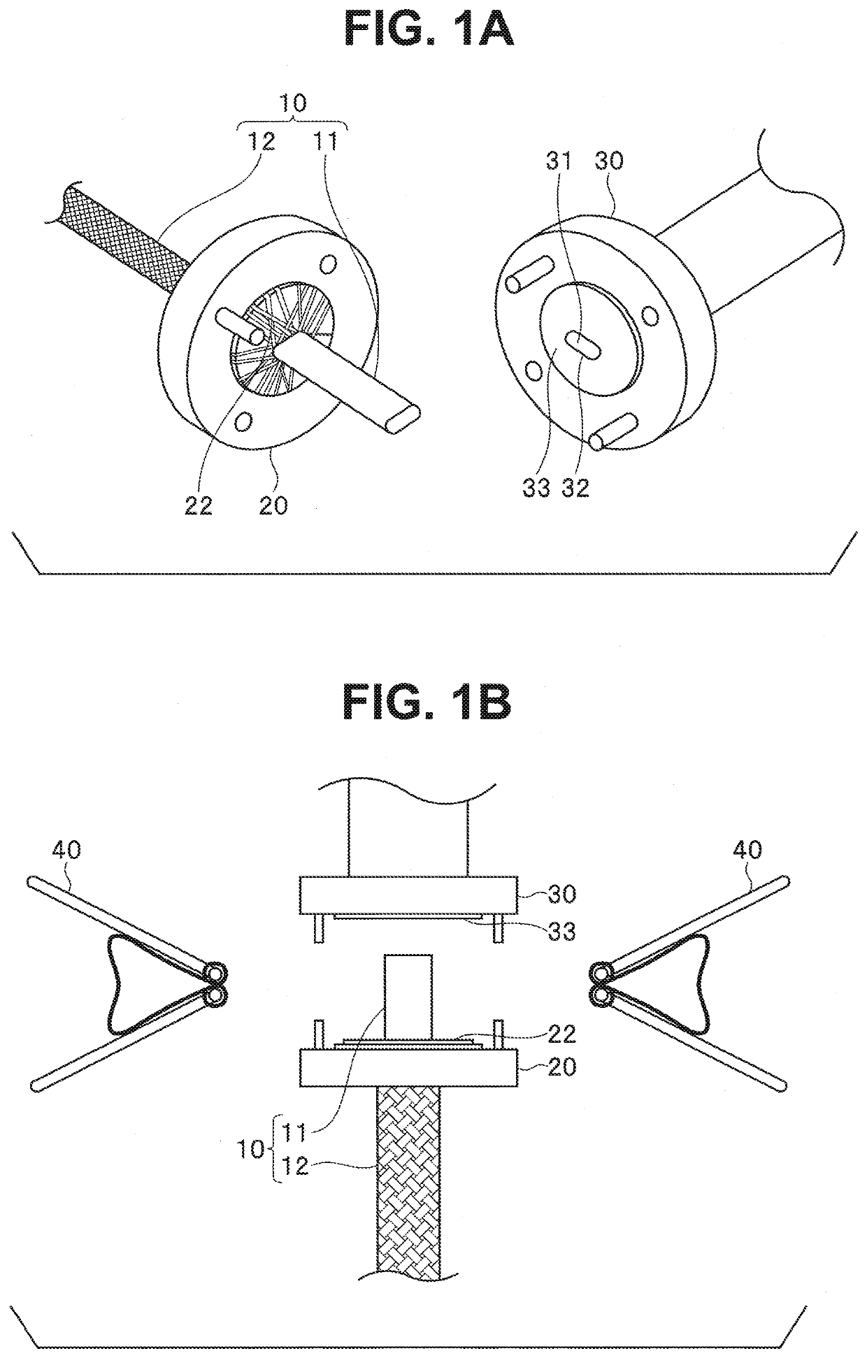
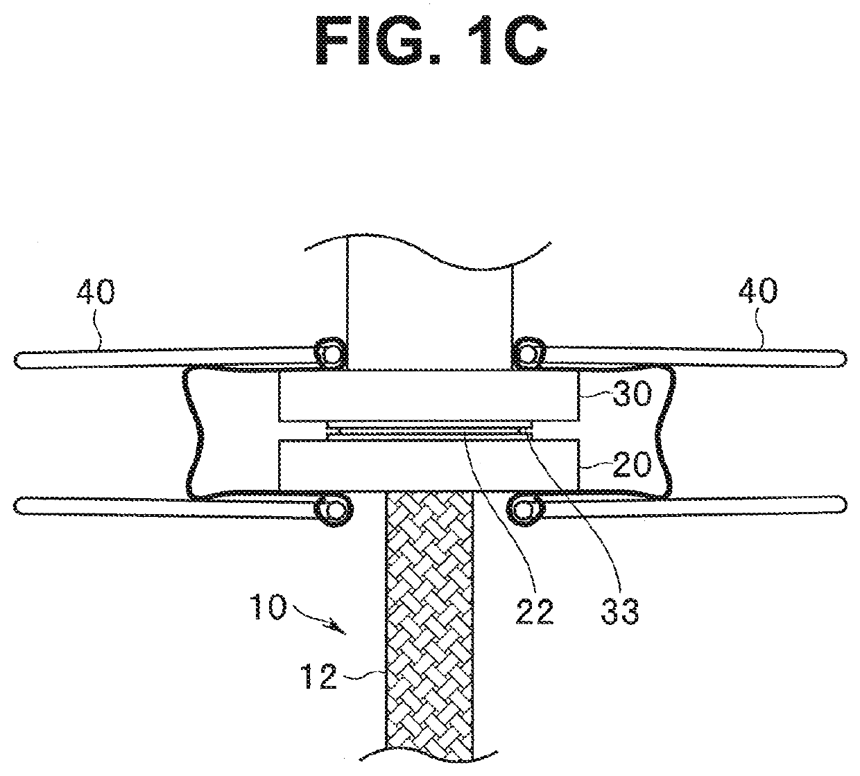
[0051]First, a configuration of a connection structure of a waveguide according to a first embodiment will be described with reference to FIG. 1 to FIG. 4. FIG. 1A is an external appearance view showing external appearances of a flexible waveguide used for transmitting radio waves in a millimeter wave band, a fixing member, and a three-dimensional component, and showing a state where an end portion of the flexible waveguide is combined with the fixing member. FIG. 1B is an external appearance view showing the external appearances of the flexible waveguide, the fixing member, the three-dimensional component, and auxiliary pressing members. FIG. 1C is an external appearance view showing an assembled state where the flexible waveguide, the fixing member, the three-dimensional component, and the auxiliary pressing members are combined with each other.

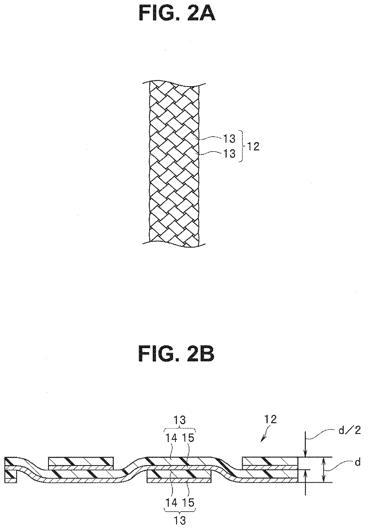
[0052]FIG. 2A is an external appearance view showing an external appearance of an outer conductor of the flexible waveguide, the outer con...

second embodiment

[0082]Next, a second embodiment will be described.

[0083]FIG. 5 is a cross-sectional view showing a cross sections of a flexible waveguide, a fixing member, and a three-dimensional component of the second embodiment in a combined state.

[0084]As shown in FIG. 5, an insertion hole 31 of a three-dimensional component 30 in the present embodiment has a tapered structure where the diameter increases from a surface through which the dielectric 11 is inserted toward an opening 36 on the opposite side. By setting the major axis “A” and the minor axis “B” of the insertion hole 31 on the connection surface 33 side to be substantially equal to the major axis “a” and the minor axis “b” of the dielectric 11, the flexible waveguide 10 and the three-dimensional component 30 can be easily connected with each other.

[0085]The distal end (end portion) of the dielectric 11 has a pointed shape, that is, a shape in which the cross-sectional area of the dielectric 11 gradually decreases, in the insertion h...

third embodiment

[0097]Next, a third embodiment will be described.

[0098]In the third embodiment, the description will be made with respect to a waveguide connector for connecting the flexible waveguide 10 to another device, such as a measuring instrument.

[0099]FIG. 14A is an external appearance view showing external appearances of a flexible waveguide, a fixing member, a three-dimensional component, and auxiliary pressing members, and showing a state where the end portion of the flexible waveguide is combined with the fixing member. FIG. 14B is an external appearance view showing a state before the fixing member is combined with the three-dimensional component.

[0100]As shown in FIG. 14A and FIG. 14B, a waveguide connector 60 of the present embodiment is configured of a flexible waveguide 10, a fixing member 20, a three-dimensional component 30, and auxiliary pressing members 40. A connection surface 33 of the three-dimensional component 30 has a tapered structure where the connection surface 33 prot...


PUM

PropertyMeasurementUnit
wavelengthaaaaaaaaaa
sizeaaaaaaaaaa

Abstract

A connection structure of a waveguide includes a rod-like dielectric, and an outer conductor. A three-dimensional component includes a connection surface, an insertion hole, and a corner which forms an opening edge of the insertion hole over an entire circumference on the connection surface, the connection surface at least partially including a conductive region to which a connection enlarged portion of the outer conductor is connected, the insertion hole having conductivity over an entire circumference of an inner surface, the corner having conductivity and being conducted with the inner surface of the insertion hole. In a state where the waveguide and the three-dimensional component are connected with each other, the connection enlarged portion is electrically conducted with the inner surface of the insertion hole through electrical connection with the connection surface and the corner, and smooth connection is made at the corner.

Description

CROSS REFERENCE TO RELATED APPLICATION[0001]This application is a continuation application of PCT / JP2020 / 037991 filed on Oct. 7, 2020 and claims benefit of Japanese Application No. 2019-233391 filed in Japan on Dec. 24, 2019, the entire contents of which are incorporated herein by this reference.BACKGROUND OF THE INVENTION1. Field of the Invention[0002]The present invention relates to a connection structure of a waveguide, a waveguide connector, a mode converter, and a waveguide unit, and particularly to a connection structure of a waveguide including an outer conductor having a braid shape, a waveguide connector, a mode converter, and a waveguide unit.2. Description of the Related Art[0003]In recent years, in various fields including the field of broadcasting, an effort has been widely made to achieve high definition video, such as 4K / 8K images. High definition video, such as 4K / 8K images, has a large video information volume due to the increase in the number of pixels and hence, a...

Claims


Application Information

Patent Timeline
Patent Type & Authority Applications(United States)
IPC IPC(8): H01P5/08H01P3/12H01P3/16
CPCH01P5/08H01P3/12H01P3/16H01P1/04H01P3/14H01P1/16H01P1/042H01P3/122
Inventor WATANABE, TADASHISUESADA, SHINJI
Owner OLYMPUS CORP
Why Eureka
Try Eureka