Non-linear optical thin film, non-linear optical device using the same, and optical switch using the same

a technology of optical thin film and nonlinear optical device, applied in nonlinear optics, instruments, optics, etc., can solve problems such as signal attenuation, and achieve the effects of reducing loss, good switching characteristics, and reducing loss

Inactive Publication Date: 2005-05-31
HITACHI LTD
View PDF4 Cites 2 Cited by
  • Summary
  • Abstract
  • Description
  • Claims
  • Application Information

AI Technical Summary

Benefits of technology

[0007]According to the present invention that solves the above-mentioned problem, there is provided a thin film comprising oxide particles having a corundum type crystal structure and amorphous grain boundaries in the surroundings of the oxide particles. The corundum type structure means a structure in which one more kind of atom is contained in a vacancy in a hexagonal crystal, which can be distinguished by a diffraction image obtained by a TEM (transmission electron microscope) or wide angle X-rays. Such a thin film has a refractive index variation sufficient for application to optical devices, and shows little loss of signals.
[0008]When having a mean particle diameter of not more than 25 nm, the oxide particles provide good switching characteristics. The oxide particles, which contain aluminum oxide, iron oxide or gallium oxide, are suitable since they further reduce the loss. In addition, iron oxide is suitable since it increases a variation in refractive index of the thin film. The material oxide constituting the oxide particles can be added in a weight ratio of from 30%, inclusive, to 95%, exclusive, based on the total weight of the thin film.

Problems solved by technology

The optical switch using the thin film as above-mentioned has posed a problem that at the time of changeover of a signal optical path, absorption and / or scattering due to the thin film occurs, causing the attenuation of the signal.

Method used


Image

  • Non-linear optical thin film, non-linear optical device using the same, and optical switch using the same
  • Non-linear optical thin film, non-linear optical device using the same, and optical switch using the same
  • Non-linear optical thin film, non-linear optical device using the same, and optical switch using the same

Examples


example 1

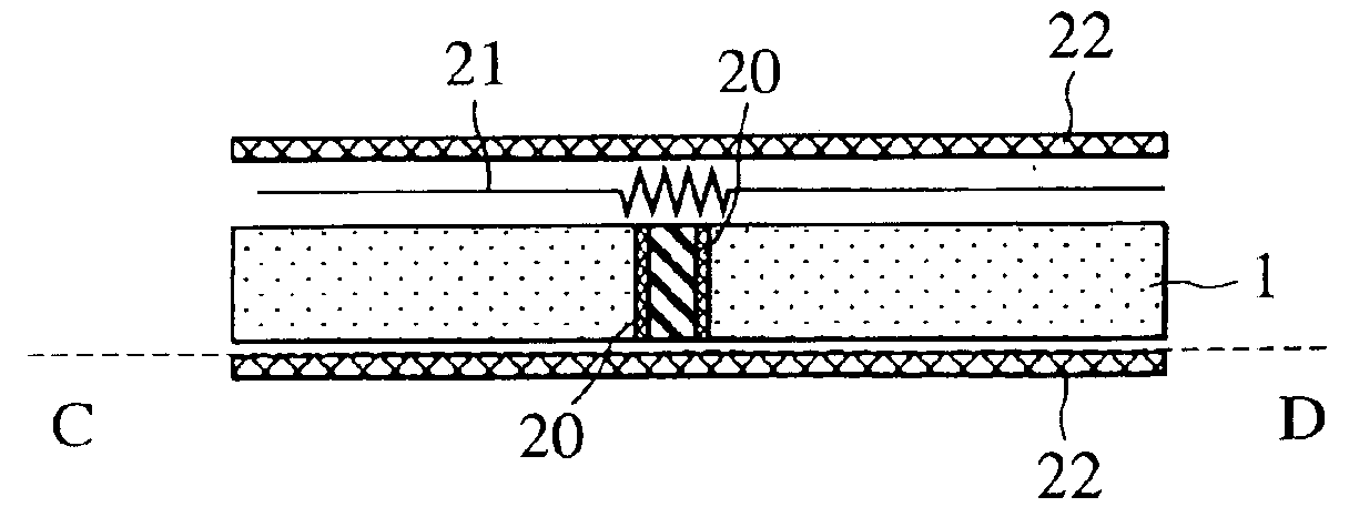
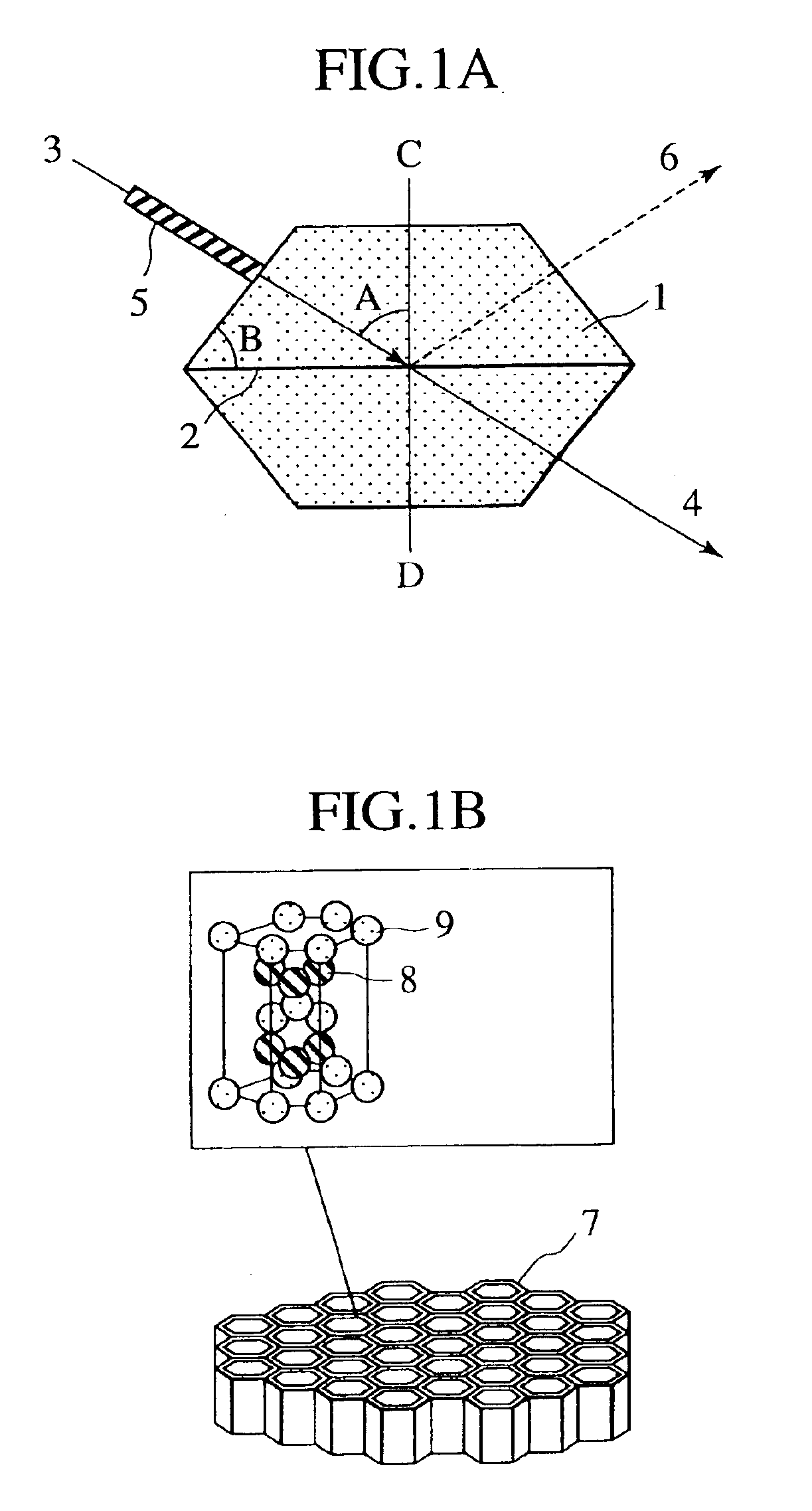
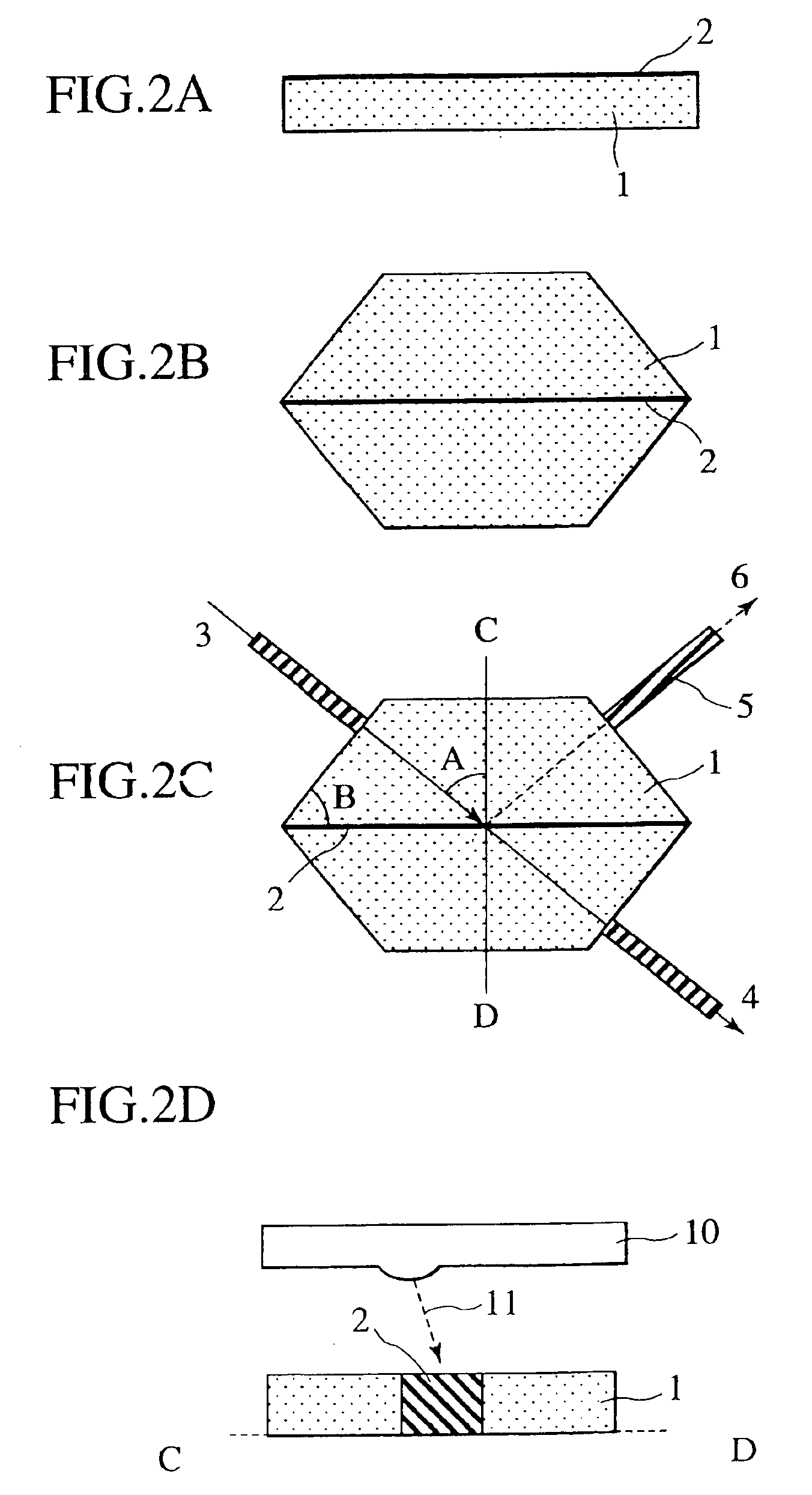
[0029]FIGS. 1A and 1B show a device for carrying out this example and a thin film used for the device, respectively. FIG. 1A is a schematic diagram showing a device structure investigated, and FIG. 1B is a schematic diagram showing a non-linear optical thin film used for the device, which comprises an oxide having the corundum type crystal structure and an amorphous oxide component. In the figures, numeral 1 denotes a glass substrate, 2 denotes a non-linear optical film comprising a metallic oxide and an amorphous oxide forming grain boundary portions thereof, 3 denotes signal light, 4 and 6 denote emitted light, 5 denotes a fiber, 7 denotes the amorphous portion, 8 denotes an oxygen atom, and 9 denotes a metal atom. In addition, character A denotes the angle of incidence of signal light, and B denotes the inclination angle of the substrate.

[0030]The glass substrate 1 was obtained by doping quartz glass with titanium oxide, and so conditioning as to obtain a refractive index of 1.65...

example 2

[0056]The non-linear optical thin film in Example 1 was obtained by growing crystal grains in a columnar shape. When the crystal grains are grown in a columnar form from the substrate, a great optical anisotropy results. Now, the results of the case where a non-linear optical thin film was grown obliquely, for investigation of the anisotropy of the film, will be shown below. FIG. 6 illustrates the method of growth, in which numeral 19 denotes a sputter target, and 1 denotes a glass substrate. As shown in the figure, the non-linear optical thin film was grown with the substrate inclined by an angle of 5°.

[0057]When a cross section of the thin film portion thus formed was observed under a TEM (transmission electron microscope), it was observed that the thin film had been grown obliquely relative to the substrate, and it was confirmed that the direction of growth coincided with the inclination angle of 5°. An optical device was produced by application of the above-described production ...

example 3

[0064]An optical switch was produced by use of a non-linear optical device. Irradiation with laser light from a planar emission laser was conducted together with changeover information written in a light signal. The length of the changeover information was set to 20 ns, which corresponds to an ordinary data transfer speed at present. As a result, it was found that the optical path of the input light was changed over based on the changeover information.

[0065]As described above, use of the thin film according to the present invention makes it possible to produce a device that can perform changeover or turning-ON / OFF of optical path efficiently and with low loss. While the changeover of optical path was evidenced in this example, it is possible to use the optical device as an optical shutter or a fuse, by absorbing the output light in either direction of the emission optical paths 4 and 6 by use of a filter for absorbing the light.


PUM

PropertyMeasurementUnit
mean particle diameteraaaaaaaaaa
wavelengthaaaaaaaaaa
signal transmittanceaaaaaaaaaa

Abstract

An optical device is capable of changing signal light to a plurality of paths. The device includes a film, a heating source attached to the film, and a heat radiator plate attached to the other portion of the film. The refractive index of the film varies according to heat excitation, and the film comprises crystal grains of an oxide and amorphous portions present between the crystal grains.

Description

[0001]This application is a Continuation of Ser. No. 10 / 378,863 filed Mar. 5, 2003, now U.S. Pat. No. 6,804,043.BACKGROUND OF THE INVENTION[0002]The present invention relates to a non-linear optical film having a non-linear optical characteristic for use in a device for changeover of a signal optical path or for turning-ON / OFF of a signal.[0003]The conventional switching of light information has required a photo-electric conversion means for once converting light information into electrical information and an electro-photo conversion means for reversely converting the electrical information into light information at each relay point. In order to build up a higher-speed light communication system, optical switches (mechanical type optical switches, planar light waveguide type optical switches, mirror type optical switches, bubble type switches, etc.) for directly switching the light information have been developed as described in “Nikkei Electronics” No. 8, Jan. 29, 2000 (non-patent ...

Claims


Application Information

Patent Timeline
Patent Type & Authority Patents(United States)
IPC IPC(8): G02F1/355G02F1/35
CPCG02F1/3551G02F1/35
Inventor HONDA, MITSUTOSHISAWAI, YUICHIMOMOSE, HIDETOAKATA, HIROYUKINAITO, TAKASHI
Owner HITACHI LTD
Why Eureka
Try Eureka