Fan-out Packaging Method and Fan-out Packaging Plate

a packaging method and fan-out technology, applied in the field of electronic devices, can solve the problems of incompatibility between the two processes, affecting the receipt and transmission of high-frequency signals in the packaged device, and relatively poor high-frequency electrical performance of the thermosetting material, so as to reduce the dissipation factor of the packaging material and small signal loss

Active Publication Date: 2022-02-17
SHENZHEN XIUYI INVESTMENT DEV PARTNERSHIP LLP
View PDF7 Cites 4 Cited by
  • Summary
  • Abstract
  • Description
  • Claims
  • Application Information

AI Technical Summary

Benefits of technology

[0003]In view of this, the present disclosure aims at providing a fan-out packaging method and a fan-out packaging plate to overcome the defects in the prior art, which reduces the dissipation factor of the packaging material, has small signal loss, and can be well applied to the packaging of high-frequency radio-frequency devices.

Problems solved by technology

Such type of thermosetting material has relatively poor high-frequency electrical performance and a large dissipation factor (or loss tangent), and then will cause large signal loss in a high-frequency section, thereby affecting receipt and transmission of high-frequency signals in a packaged device.
The conventional thermoplastic material packaging process is used in cooperation with the conventional flip-chip fan-out process, and if it is replaced with the packaging method of the present disclosure, it is quite easy to cause incompatibility of the two processes, and the fan-out and packaging cannot be completed.

Method used


Image

  • Fan-out Packaging Method and Fan-out Packaging Plate
  • Fan-out Packaging Method and Fan-out Packaging Plate
  • Fan-out Packaging Method and Fan-out Packaging Plate

Examples


embodiment 1

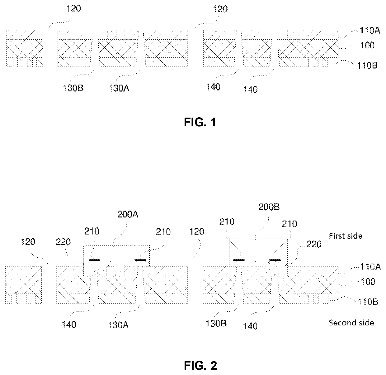
[0056]As shown in FIGS. 1 to 7, in the present embodiment, packaging layers are fabricated simultaneously on two sides of a substrate for packaging, but it is not limited thereto, while a method of the present disclosure further may be used for packaging only a single side of the substrate.

[0057]As shown in FIG. 1, circuit patterns 110A and 1108 are fabricated on two sides of a substrate 100, and the circuit patterns 110A and 1108 on the two sides of the substrate 100 may be electrically connected to each other or not. The circuit patterns 110A and 1108 include, but are not limited to, wirings, interconnection lines, antennas, and pins with electronic functionality, and the materials for fabricating the circuit patterns 110A and 1108 include, but are not limited to, copper, or silver, or iron, or other conductive materials or semiconductor materials. Via holes 120, external connection holes 140 and interconnection holes 130A and 1308 are fabricated on the substrate 100.

[0058]As show...

embodiment 2

[0068]Embodiment 2 differs from Embodiment 1 in that:

[0069]the electronic parts 200A and 200B are thinned and then packaging is carried out.

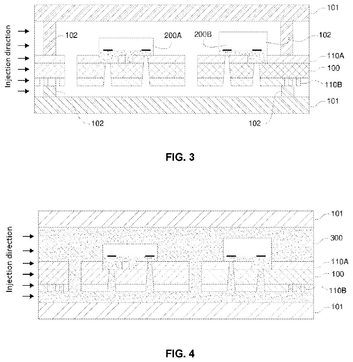
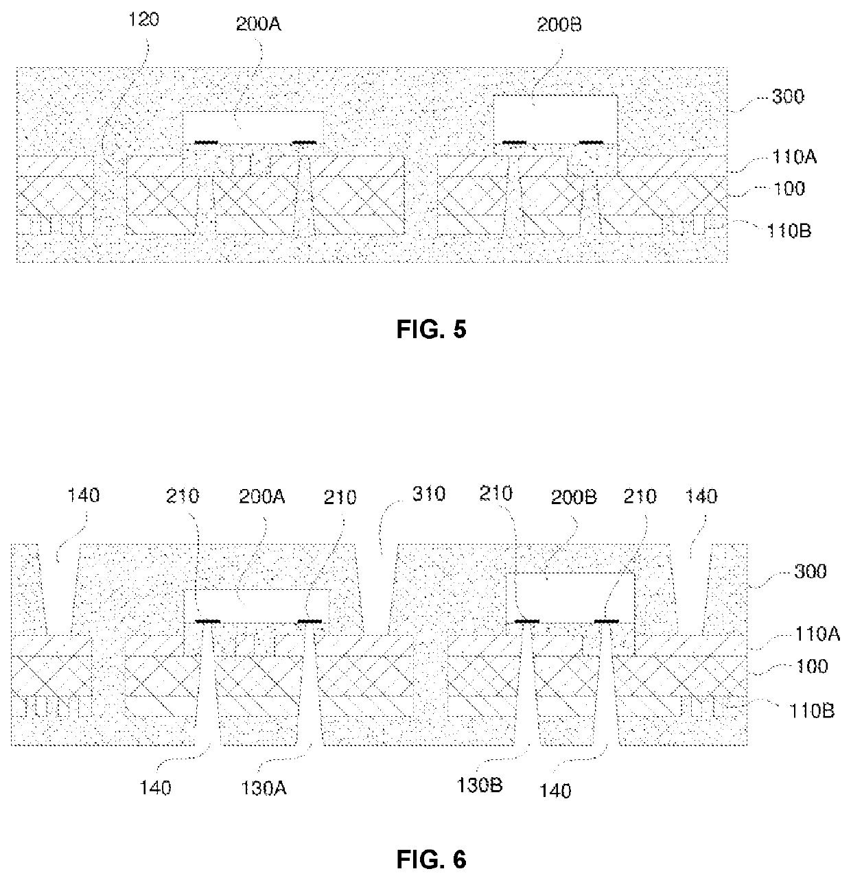
[0070]As shown in FIG. 8, the circuit patterns 110A and 1108 are fabricated on the two sides of the substrate 100, and the via hole 120, the external connection hole 140 and the interconnection holes 130A and 130B are fabricated in the substrate 100.

[0071]As shown in FIG. 9, the electronic parts 200A and 200B are pasted to the substrate 100 by a patch material 220.

[0072]As shown in FIG. 10, after the electronic parts 200A and 200B are mounted on the substrate 100, at this time, positions of the electronic parts 200A and 200B relative to the substrate 100 are fixed, and the thicknesses (the thickness refers to height of the electronic parts protruding relative to the substrate) of the electronic parts 200A and 200B are reduced by grinding, cutting or other methods, and then the packaging layers 300 are fabricated. After the thicknesses of the ele...


PUM


Abstract

A fan-out packaging method includes: prepare circuit patterns on one side or both sides of a substrate; install electronic parts on one side or both sides of the substrate; prepare packaging layers on both sides of the substrate; the packaging layers on both sides of the substrate package the substrate, the circuit patterns, and the electronic parts, the packaging layers being made of a thermal-plastic material; wherein the substrate is provided with a via hole; both sides of the substrate are communicated by means of the via hole; a part of the packaging layers penetrate through the via hole when the packaging layers are prepared on both sides of the substrate; and the packaging layers on both sides of the substrate are connected by means of the via hole.

Description

TECHNICAL FIELD[0001]The present disclosure belongs to the electronic field, and in particular relates to a fan-out packaging method and a fan-out packaging plate.BACKGROUND ART[0002]Conventional fan-out packaging typically adopts a compression molding or transfer molding method in the outer package injection molding process, in which a thermosetting packaging material, such as epoxy, is injected into a mold and then heated to cure. Such type of thermosetting material has relatively poor high-frequency electrical performance and a large dissipation factor (or loss tangent), and then will cause large signal loss in a high-frequency section, thereby affecting receipt and transmission of high-frequency signals in a packaged device.SUMMARY[0003]In view of this, the present disclosure aims at providing a fan-out packaging method and a fan-out packaging plate to overcome the defects in the prior art, which reduces the dissipation factor of the packaging material, has small signal loss, an...

Claims


Application Information

Patent Timeline
Patent Type & Authority Applications(United States)
IPC IPC(8): H01L21/56H01L23/29H01L23/31H01L23/00
CPCH01L21/56H01L23/29H01L2224/92144H01L24/92H01L23/3107H01L24/19H01L24/20H01L2224/73217H01L2924/00014H01L2224/83385H01L24/83H01L24/73H01L2924/181H01L2924/15321H01L23/5389H01L23/5384H01L21/565H01L2224/29099H01L2924/00012
Inventor HU, CHUANYAN, YINGQIANGGUO, YUEJINPI, YINGJUNLIU, JUNJUNPRACK, EDWARD
Owner SHENZHEN XIUYI INVESTMENT DEV PARTNERSHIP LLP
Why Eureka
Try Eureka