Semiconductor device

a semiconductor device and semiconductor technology, applied in the field of semiconductor devices, can solve the problems of deterioration in the reliability of the semiconductor device, cracking or peeling of the resin, and damage to the resin,

Pending Publication Date: 2022-09-22
FUJI ELECTRIC CO LTD
View PDF0 Cites 0 Cited by
  • Summary
  • Abstract
  • Description
  • Claims
  • Application Information

AI Technical Summary

Benefits of technology

[0086]According to the disclosed techniques, the occurrence of damage is suppressed, deterioration in insulation resistance is prevented, damage to a semiconductor device is prevented, and deterioration in the reliability of a semiconductor device is suppressed.

Problems solved by technology

However, if the insulator is resin and the lead frames are disposed adjacently to each other, then damage, such as a crack or peeling, to the resin may occur.
If damage occurs to the resin used for insulating one lead frame from the other, then it may be that insulation between the lead frames is not maintained.
This may lead to deterioration in the reliability of the semiconductor device.

Method used


Image

  • Semiconductor device
  • Semiconductor device
  • Semiconductor device

Examples


first embodiment

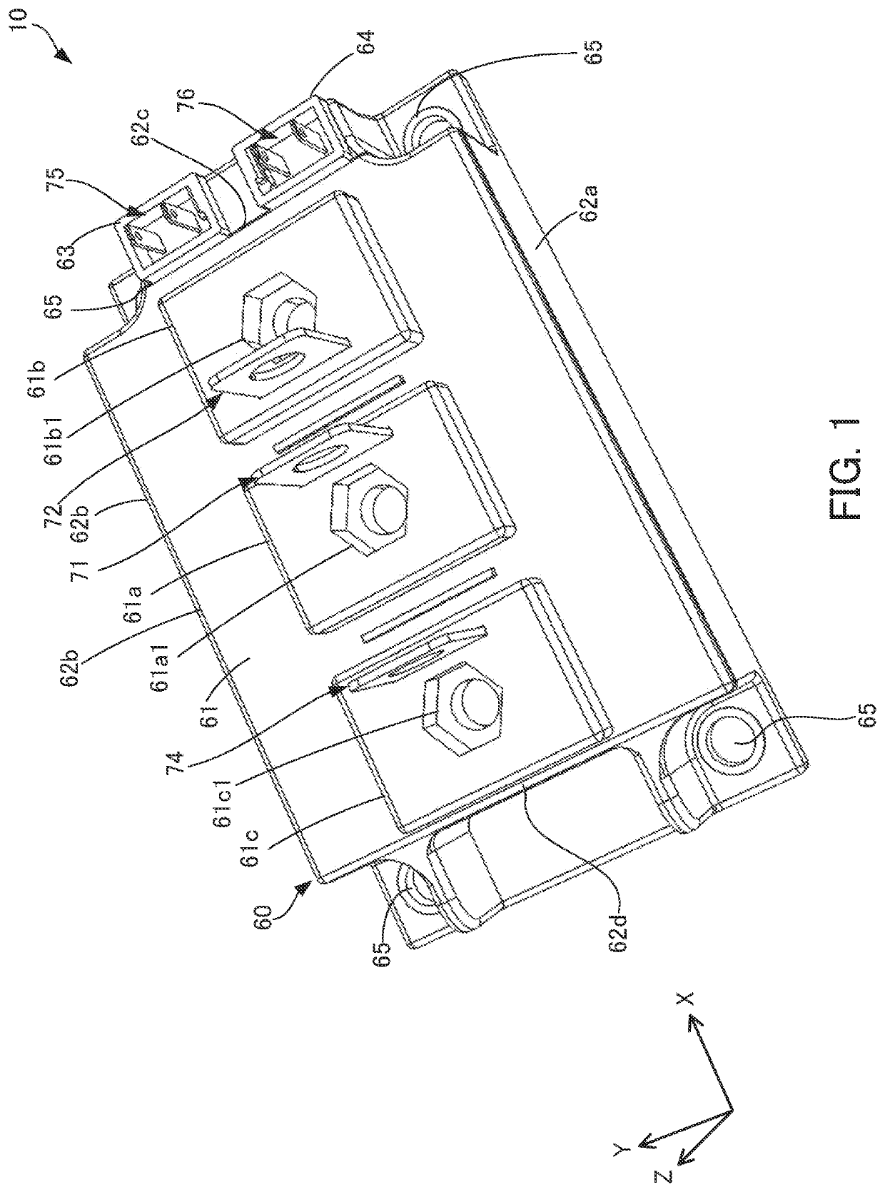
[0024]The external appearance of a semiconductor device according to a first embodiment will be described with reference to FIG. 1. FIG. 1 is an external view of a semiconductor device according to a first embodiment. As illustrated in FIG. 1, components of a semiconductor device 10 described later are covered with a case 60. A radiation plate 30 which is rectangular in a plan view is formed on the back surface of the semiconductor device 10 (on the back side of the case 60) (see FIG. 3).

[0025]The case 60 includes a lid portion 61, side wall portions 62a through 62d, and terminal openings 63 and 64. Furthermore, terminal blocks 61a, 61b, and 61c are formed in a central portion of the lid portion 61 in the longitudinal direction. Screw holes 61a1, 61b1, and 61c1 are made in the front surfaces of the terminal blocks 61a, 61b, and 61c, respectively. First, second, and third wiring members 71, 72, and 74 extend upward from the terminal blocks 61a, 61b, and 61c, respectively. FIG. 1 illu...

modification 1

[0075]Modification 1 of the wiring unit 70 will be described with reference to FIG. 9. FIG. 9 is a fragmentary sectional view of a wiring unit included in modification 1 of the semiconductor device according to the first embodiment. With a wiring unit 70 included in modification 1 of the semiconductor device according to the first embodiment, a lower surface 73a1 of a first portion 73a of a wiring holding portion 73 protrudes from back surfaces of a first horizontal portion 71a and a second horizontal portion 72a toward front surfaces of insulated circuit boards 20a and 20b (in the −Z direction in FIG. 9), compared with the wiring unit 70 illustrated in FIG. 8. A protrusion amount of the lower surface 73a1 of the first portion 73a from the back surfaces of the first horizontal portion 71a and the second horizontal portion 72a may be 50 percent or more of the distance between the principal plane of a first vertical portion 71b and the principal plane of a second vertical portion 72b ...

modification 2

[0076]Modification 2 of the wiring unit 70 will be described with reference to FIG. 10. FIG. 10 is a fragmentary sectional view of a wiring unit included in modification 2 of the semiconductor device according to the first embodiment. With a wiring unit 70 included in modification 2 of the semiconductor device according to the first embodiment, the curvature of a first bent portion 71c of a first wiring member 71 and a second bent portion 72c of a second wiring member 72 is smaller than that of the first bent portion 71c of the first wiring member 71 and the second bent portion 72c of the second wiring member 72, respectively, included in the wiring unit 70 illustrated in FIG. 8. That is to say, with the wiring unit 70 included in modification 2 of the semiconductor device according to the first embodiment, the first bent portion 71c of the first wiring member 71 and the second bent portion 72c of the second wiring member 72 curve more gently than the first bent portion 71c of the f...


PUM

PropertyMeasurementUnit
distanceaaaaaaaaaa
thicknessaaaaaaaaaa
thicknessaaaaaaaaaa

Abstract

A first wiring member bends at a first bent portion in the shape of the letter “L” in a side view and includes a first horizontal portion parallel to the principal surface of a semiconductor chip and a first vertical portion perpendicular to the first horizontal portion. A second wiring member bends at a second bent portion in a direction opposite to the first wiring member in the shape of the letter “L” in the side view and includes a second horizontal portion flush with the first horizontal portion and a second vertical portion a determined distance distant from the first vertical portion and parallel to the first vertical portion. A wiring holding portion fills a gap between the first and second vertical portions and a gap between the first and second bent portions. Therefore, stress applied to the vicinity of the first or second bent portion is relaxed.

Description

CROSS-REFERENCE TO RELATED APPLICATION[0001]This application is based upon and claims the benefit of priority of the prior Japanese Patent Application No. 2021-045452, filed on Mar. 19, 2021, the entire contents of which are incorporated herein by reference.BACKGROUND OF THE INVENTION1. Field of the Invention[0002]The embodiments discussed herein relate to a semiconductor device.2. Background of the Related Art[0003]Semiconductor devices include power devices and are used as, for example, power converters which make up inverters. The power devices are insulated gate bipolar transistors (IGBTs), power metal oxide semiconductor field effect transistors (MOSFETs), or the like. Such a semiconductor device includes semiconductor chips including power devices and a plurality of insulated circuit boards. Furthermore, such a semiconductor device includes a plurality of lead frames electrically connected to the semiconductor chips. As the frequency of a power converter becomes higher, there ...

Claims


Application Information

Patent Timeline
Patent Type & Authority Applications(United States)
IPC IPC(8): H01L23/049H01L23/373H01L23/00H01L25/18H01L25/07
CPCH01L23/049H01L23/3735H01L24/48H01L25/18H01L25/072H01L2924/10253H01L2924/10272H01L2924/13055H01L2924/13091H01L2924/12032H01L2924/12036H01L2924/3512H01L2924/35121H01L2224/48139H01L23/49562H01L23/49548H01L23/49555H01L23/49861H01L23/49811H01L23/49844H01L2224/49113H01L2224/4846H01L2224/48227H01L2924/19107H01L2924/181H01L2224/48091H01L2224/45147H01L2224/45124H01L2224/45015H01L24/45H01L2224/0603H01L24/49H01L24/06H01L2224/04042H01L2224/83801H01L2224/29101H01L2224/73265H01L24/32H01L24/29H01L24/83H01L2224/32225H01L23/053H01L23/24H01L2924/00012H01L2924/00014H01L2924/20755H01L2924/20756H01L2924/20757H01L2924/20758H01L2924/20759H01L2924/2076H01L2924/014
Inventor KANEKO, SATOSHI
Owner FUJI ELECTRIC CO LTD
Why Eureka
Try Eureka