Display device

Pending Publication Date: 2022-09-22
JAPAN DISPLAY INC
View PDF0 Cites 0 Cited by
  • Summary
  • Abstract
  • Description
  • Claims
  • Application Information

AI Technical Summary

Problems solved by technology

If the reflective structure fails to be formed to be high due to the restriction of thickness

Method used


Image

  • Display device
  • Display device
  • Display device

Examples


Example

First Embodiment

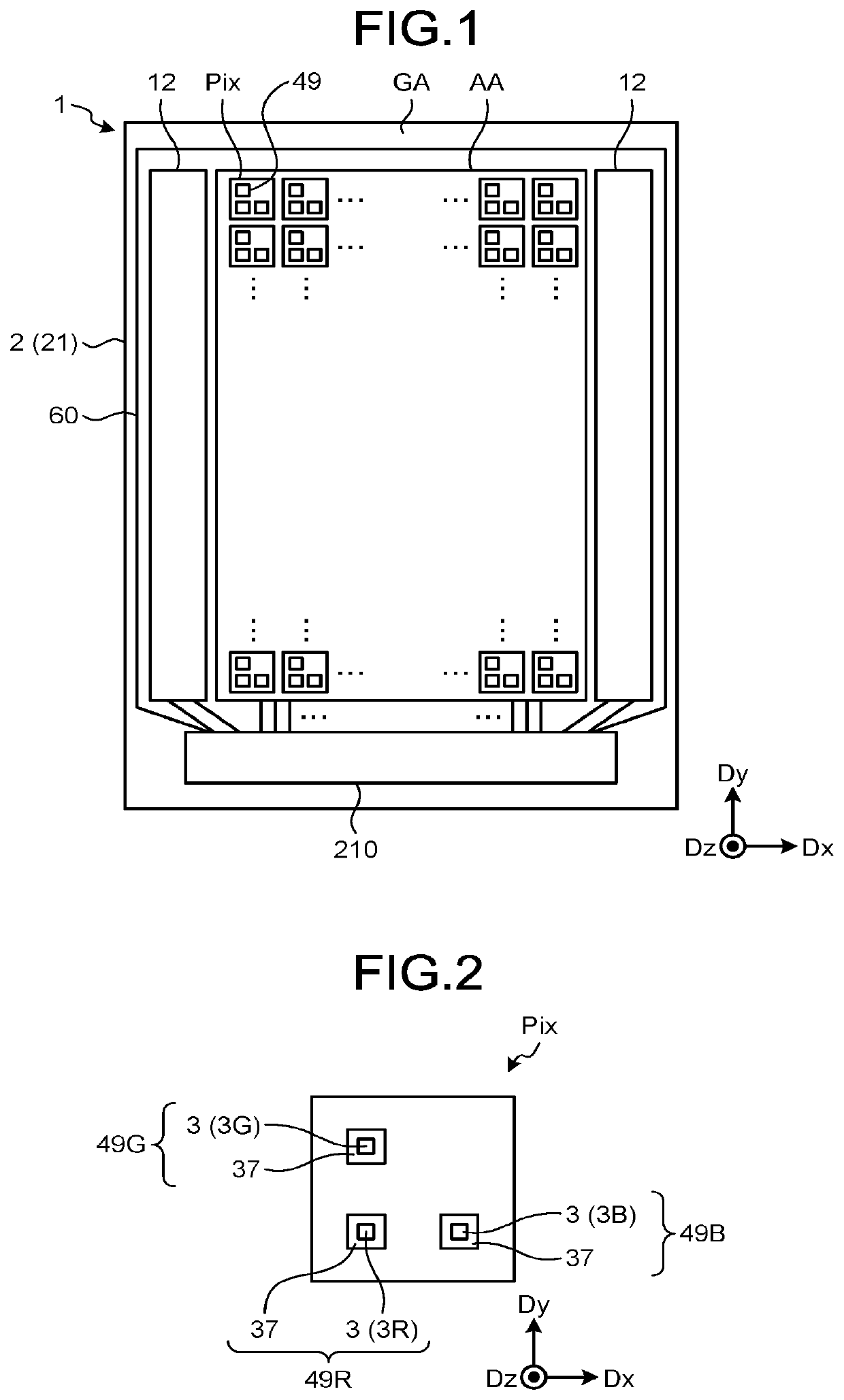
[0013]FIG. 1 is a plan view schematically illustrating a display device according to a first embodiment. As illustrated in FIG. 1, a display device 1 includes an array substrate 2, pixels Pix, drive circuits 12, a drive integrated circuit (IC) 210, and cathode wiring 60. The array substrate 2 is a drive circuit substrate that drives pixels Pix and is also called a backplane or an active matrix substrate. The array substrate 2 includes a substrate 21, a plurality of transistors, a plurality of capacitances, various kinds of wiring, and other components.

[0014]As illustrated in FIG. 1, the display device 1 has a display region AA and a peripheral region GA. The display region AA is disposed overlapping the pixels Pix and displays an image. The peripheral region GA does not overlap the pixels Pix and is positioned outside the display region AA.

[0015]The pixels Pix are arrayed in a first direction Dx and a second direction Dy in the display region AA of the substrate 21. ...


PUM


Abstract

A display device includes a substrate, a plurality of light-emitting elements and a plurality of transistors provided to the substrate, a first organic insulating film that is provided covering the transistors and is in direct contact with at least one of a source electrode and a drain electrode of the transistors, an anode electrode provided on the first organic insulating film and electrically coupled to each of the light-emitting elements, a cavity formed in the first organic insulating film and recessed toward the substrate, and a reflective layer provided covering a side and a bottom of the cavity formed in the first organic insulating film

Description

CROSS-REFERENCE TO RELATED APPLICATION[0001]This application claims the benefit of priority from Japanese Patent Application No. 2021-047647 filed on Mar. 22, 2021, the entire contents of which are incorporated herein by reference.BACKGROUND1. Technical Field[0002]The present invention relates to a display device.2. Description of the Related Art[0003]Display devices provided with micro-sized light-emitting diodes (micro LEDs) as display elements have been attracting attention. To improve the light extraction efficiency, display devices provided with light-emitting diodes include a reflective structure that reflects light output from the side surfaces of the light-emitting diode toward the display surface (refer to U.S. Pat. No. 9,876,000, Japanese Patent Application Laid-open Publication No. 2020-080361, and Masaya Tamaki, et al., “A 3.9-inch LTPS TFT Full Color MicroLED Display with Novel Driving and Reflector Cavity Process”, SID 2020 Digest, 2020; pp. 112-114, for example).[0004...

Claims


Application Information

Patent Timeline
IPC IPC(8): H01L25/16H01L33/60H01L27/12H01L23/00
CPCH01L25/167H01L33/60H01L27/124H01L27/1248H01L24/05H01L24/02H01L27/1255H01L24/32H01L2224/32145H01L2924/12041H01L2224/05548H01L2224/05569H01L2224/05624H01L2224/05639H01L2224/02331H01L2224/0239H01L2224/02381H01L2224/02375H01L2224/0235H01L33/62H01L25/0753H01L33/405H01L33/44
Inventor IKEDA, MASANOBUTANAKA, YOSHINORIHIROSAWA, JIN
Owner JAPAN DISPLAY INC
Why Eureka
Try Eureka