
Contactless connector and contactless connector assembly

a technology of contactless connectors and connector assemblies, which is applied in the direction of optical elements, circuit optical details, instruments, etc., can solve the problems of low signal transmission rate, and low signal transmission rate, and achieve the effect of small loss and stable signal transmission

Inactive Publication Date: 2022-09-22
FOXCONN (KUNSHAN) COMPUTER CONNECTOR CO LTD +1
View PDF73 Cites 0 Cited by
  • Summary
  • Abstract
  • Description
  • Claims
  • Application Information

AI Technical Summary

Benefits of technology

The present invention relates to a contactless connector and assembly that uses light for signal transmission between connectors, resulting in small signal loss and stable transmission. The contactless connector assembly can be used in various fields.

Problems solved by technology

Conductive paths on circuit board and metal cables have limitations for high-speed, high-frequency signal transmission.
As the signal rate increases, so does the loss of high-speed signals in the board and cable.
The mutual contact between the terminals will also cause wear between the terminals, resulting in poor contact.

Method used


Image

  • Contactless connector and contactless connector assembly
  • Contactless connector and contactless connector assembly
  • Contactless connector and contactless connector assembly

Examples


first embodiment

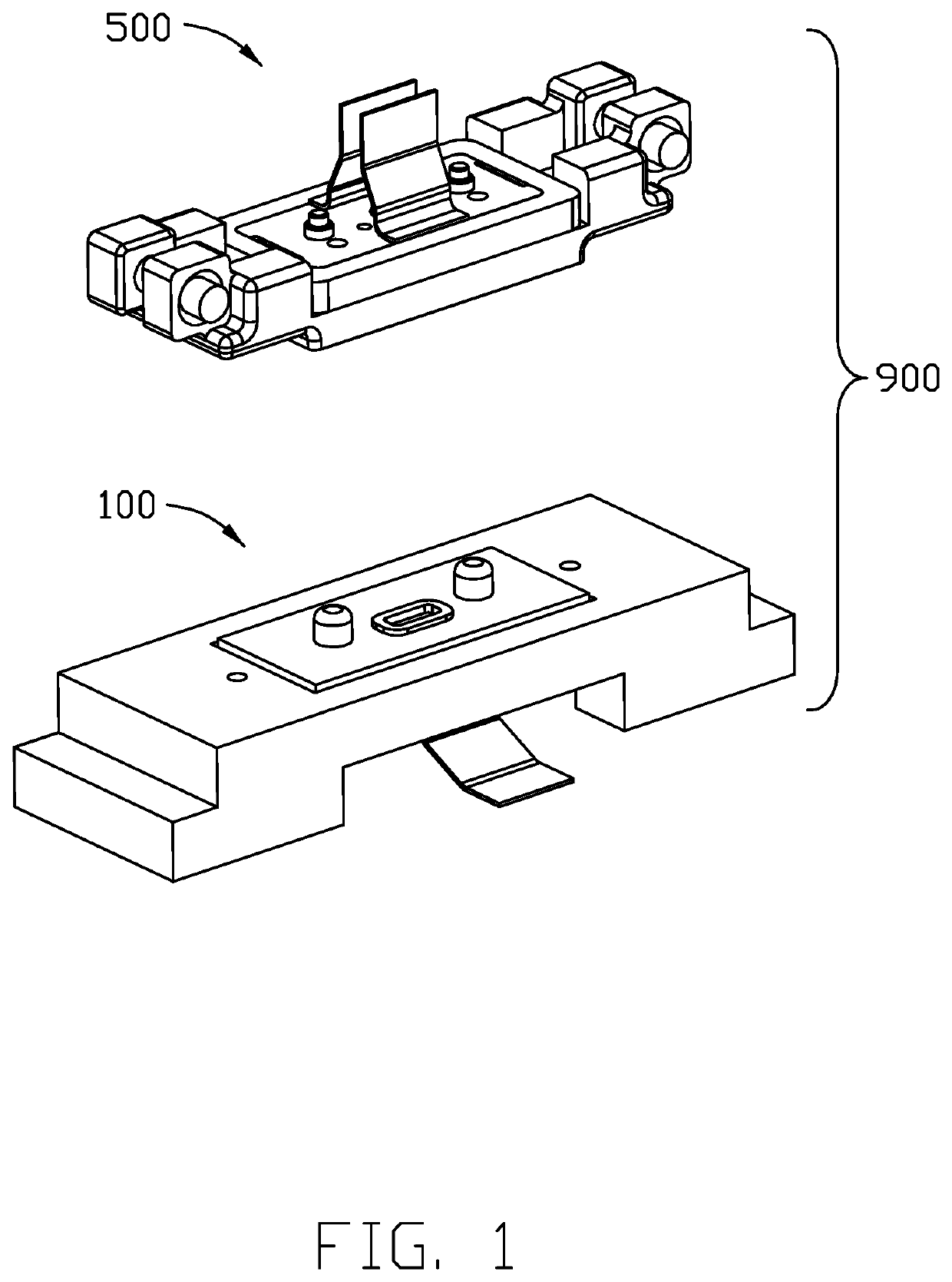
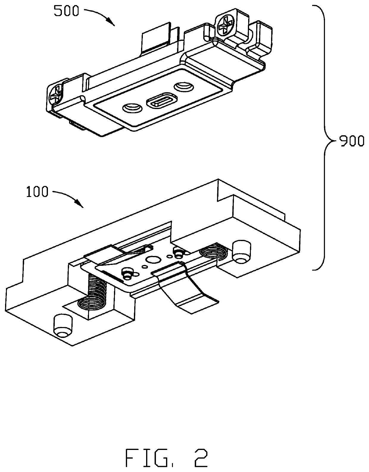
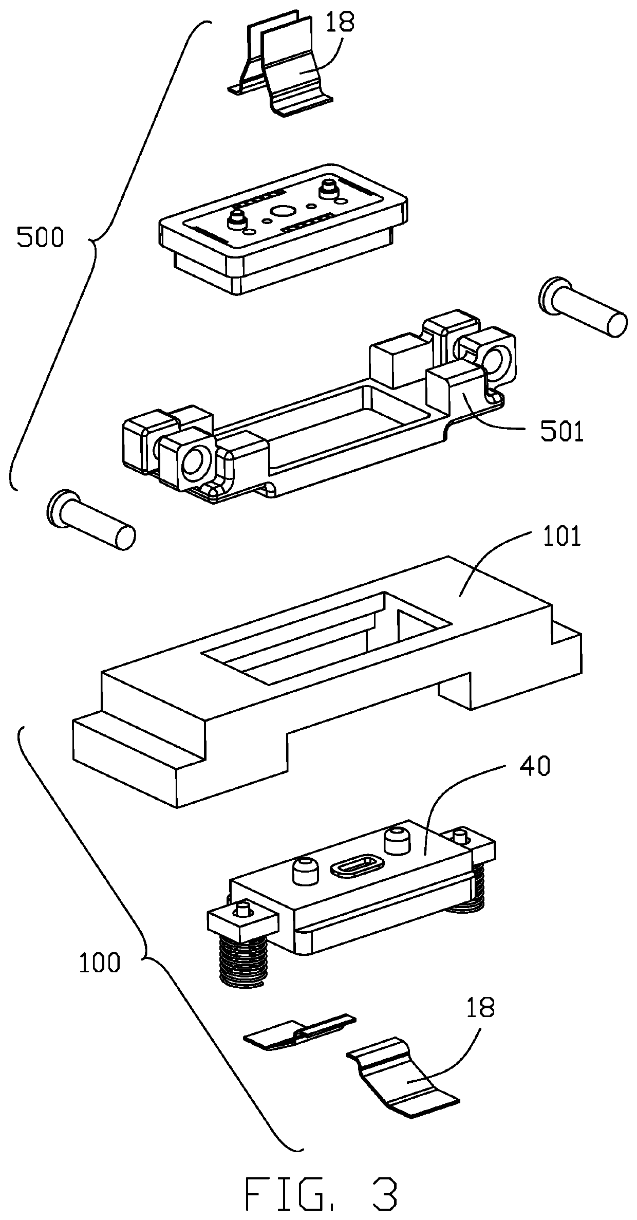
[0033]Referring to FIGS. 11-13, the contactless connector assembly 900 of the present invention further includes a sensing device that can start its operating mode. FIG. 11 shows a schematic diagram of the sensing device starting its working mode. For ease of understanding, in this embodiment, the lower connector is the first contactless connector 100 and the upper connector is the second contactless connector 500. The sensing device includes two magnetically opposed magnets 911 located on the first contactless connector 100 and the second contactless connector 500, and a Hall sensor 912 located between the magnets 911. The Hall sensor 912 senses the magnetic field formed between the two magnets when the first contactless connector 100 and the second contactless connector 500 are close to each other to start the contactless connector assembly 900 to work.

[0034]FIG. 12 shows a schematic diagram of a second embodiment of the sensing device starting its working mode. Compared with the ...

third embodiment

[0035]FIG. 13 shows a schematic diagram of the sensing device starting its working mode. In this embodiment, the sensing device includes an emitter 924 that can emit light, a receiver 925 that can receive light and a reflective element 926 that can reflects light from the emitter 924. The emitter 924 and the receiver 925 are on the first contactless connector 100, and the reflective element 926 is on the second contactless connector 500. The receiver 925 can receive the light reflected back by the reflective element 926. Of course, the emitter 924 and the receiver 925 can also be located on the second contactless connector 500, and the reflective element 926 can be located on the first contactless connector 100. The receiver 925 receives the light reflected by the reflective element 926 when the first contactless connector 100 and the second contactless connector 500 are close to each other to start the contactless connector assembly 900 in working condition

[0036]The contactless con...


PUM

PropertyMeasurementUnit
wavelengthaaaaaaaaaa
heightaaaaaaaaaa
widthaaaaaaaaaa

Abstract

A contactless connector includes: a circuit board; a light emitter arranged on the circuit board and capable of converting electrical signals into optical signals; a light emitter control chip arranged on the circuit board for controlling the operation of the light emitter; and a light-transmitting member at least partially covering the circuit board, the light emitter, and the light emitter control chip.

Description

BACKGROUND OF THE INVENTION1. Field of the Invention[0001]The present invention relates generally to a contactless connector and a contactless connector assembly including the contactless connector, and more particularly to a contactless connector and a contactless connector assembly capable of transmission of light signal.2. Description of Related Arts[0002]In one traditional design, the transmission of signals between two connectors is usually achieved through the mutual contact of their terminal, or through conductive paths on the circuit board, or metal cables. Conductive paths on circuit board and metal cables have limitations for high-speed, high-frequency signal transmission. As the signal rate increases, so does the loss of high-speed signals in the board and cable. The mutual contact between the terminals will also cause wear between the terminals, resulting in poor contact.[0003]Improved contactless connector and contactless connector assembly are desired.SUMMARY OF THE IN...

Claims


Application Information

Patent Timeline
Patent Type & Authority Applications(United States)
IPC IPC(8): H04B10/50G02B27/30G02B19/00H05K1/02H04B10/11
CPCH04B10/501G02B27/30G02B19/0009G02B19/0047H05K1/0274H04B10/11H05K2201/08H05K2201/10121H05K2201/10151G01R33/07G02B6/428G02B6/3897G01R33/072G02B6/4292G02B6/4204G02B6/4281G02B6/3886H04B10/803
Inventor XU, HAI-JUNLIN, TUNG-LOU
Owner FOXCONN (KUNSHAN) COMPUTER CONNECTOR CO LTD
Learn More