Semiconductor laser apparatus

a laser and semiconductor technology, applied in semiconductor lasers, electrical devices, laser details, etc., can solve the problems of small loss, increase in scattering loss, and absorption loss of light of fundamental modes, and achieve the effect of improving light outpu

Inactive Publication Date: 2009-05-14
SONY CORP
View PDF2 Cites 3 Cited by
  • Summary
  • Abstract
  • Description
  • Claims
  • Application Information

AI Technical Summary

Benefits of technology

[0008]Light of a higher-order mode as thus described can be generated as a result of an increase in the thickness of the region of layers to serve as an optical waveguide, and this is a characteristic unique to semiconductor laser apparatus having an LOC structure. Light of a higher-order mode results in a light intensity distribution which is more dispersed than that obtained from light of a fundamental mode, and it may constitute a factor which can degrade a characteristic desired for a semiconductor laser apparatus having an LOC structure, i.e., improved light output.
[0009]In this regard, as described in Non-Patent Document 1, the thickness of clad layers may be decreased to increase loss of light of a higher-order mode attributable to scattering of the same out of an optical waveguide, whereby the light of a higher-order mode can be suppressed. This is a method of suppressing oscillation of light of a higher-order mode by imparting greater loss to the higher-order mode utilizing the fact that light of a higher-order mode has more components bleeding through and exiting an optical waveguide compared to light of a fundamental mode. However, such a method also results in increases in scattering loss and absorption loss of light of a fundamental mode, although the loss is small. As a result, according to the method, desired characteristics of a semiconductor laser apparatus having an LOC structure can be degraded.
[0013]According to the embodiment of the invention, even when a layer serving as an optical waveguide is formed with such a thickness that not only light of a fundamental mode but also light of a higher-order mode is guided, the oscillation of the light of a higher-order mode is suppressed by forming an absorption layer. On the other hand, the light of a fundamental mode does not undergo oscillation beyond a required level and suffers from substantially no loss of light intensity as a result of the formation of the absorption layer. It is therefore possible to achieve improved light output that is a desirable characteristic unique to an LOC structure while suppressing oscillation of the light of a higher-order mode.

Problems solved by technology

However, such a method also results in increases in scattering loss and absorption loss of light of a fundamental mode, although the loss is small.

Method used


Image

  • Semiconductor laser apparatus
  • Semiconductor laser apparatus
  • Semiconductor laser apparatus

Examples


Embodiment Construction

[0019]A semiconductor laser apparatus according to an embodiment of the invention will now be described with reference to the drawings.

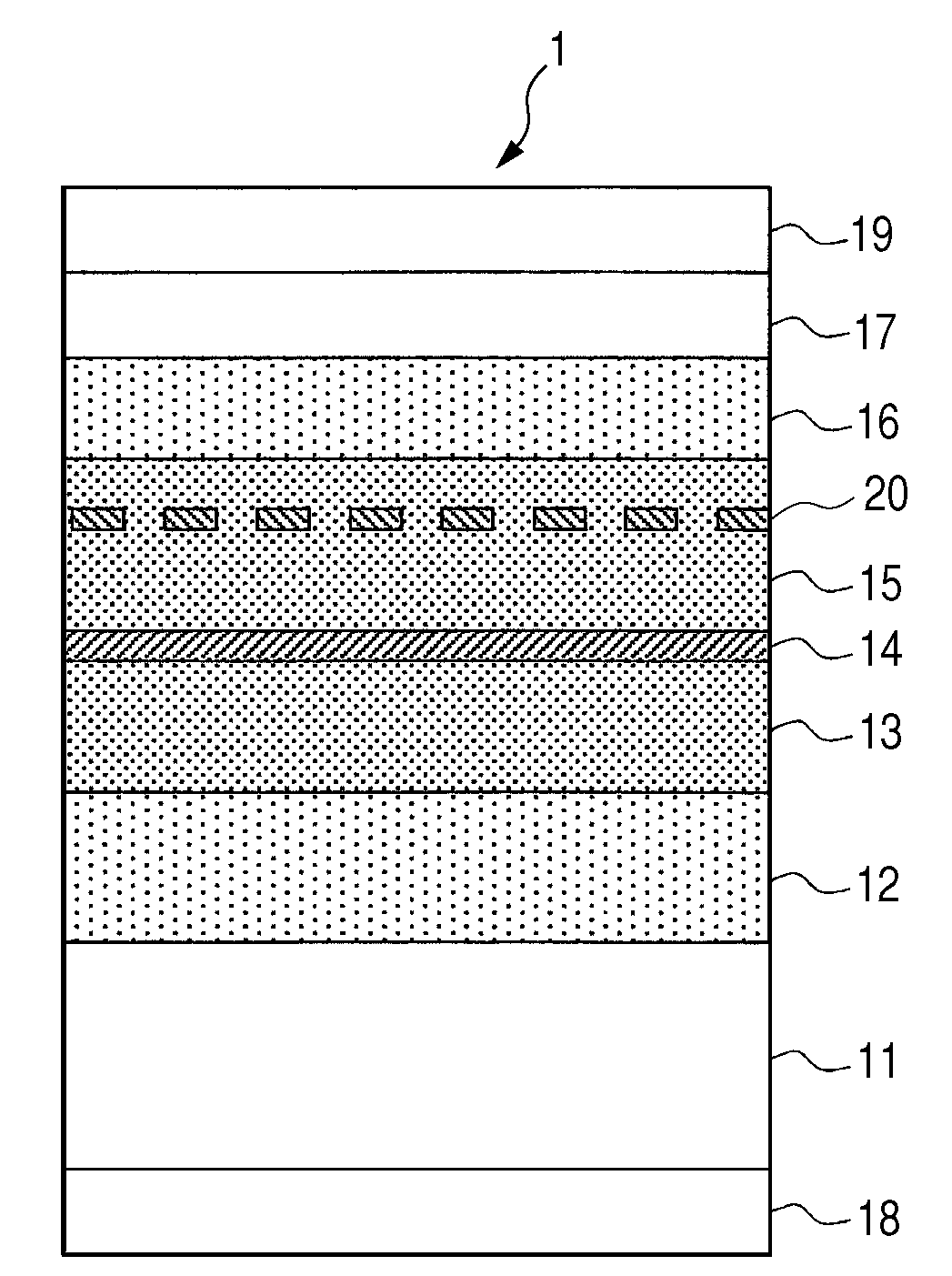
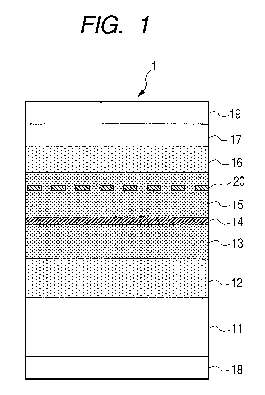
[0020]FIG. 1 is an illustration showing an exemplary configuration of a multi-layer structure of a semiconductor laser apparatus 1 according to an embodiment of the invention. The semiconductor laser apparatus 1 described here has a multi-layer structure as illustrated to serve as a semiconductor crystal element section for emitting light. Specifically, the apparatus has a multi-layer structure provided by forming an n-clad layer 12 to serve as a first clad layer, an n-guide layer 13 to serve as a first guide layer, an active layer 14, a p-guide layer 15 to serve as a second guide layer, a p-clad layer 16 to serve as a second clad layer, and a contact layer 17 in the order listed on a substrate 11. The apparatus further includes a negative electrode 18 and a positive electrode 19 disposed to sandwich the multi-layer structure.

[0021]For example, an n-...


PUM


Abstract

A semiconductor laser apparatus having a first clad layer, a first guide layer, an active layer, a second guide layer, and a second clad later formed in the order listed is disclosed. A layer serving as an optical waveguide is formed between the first clad layer and the second clad layer and wherein the layer serving as an optical waveguide is formed with such a thickness that not only light of a fundamental mode but also light of a higher-order mode is guided. An absorption layer absorbing the light of a higher-order mode is formed in a position to suppress only the oscillation of the light of a higher-order mode, the absorption layer being formed as a layer forming part of the layer to serve as an optical waveguide.

Description

CROSS REFERENCES TO RELATED APPLICATIONS[0001]The present invention contains subject matter related to Japanese Patent Application JP 2007-283156 filed in the Japanese Patent Office on Oct. 31, 2007, the entire contents of which being incorporated herein by reference.BACKGROUND OF THE INVENTION[0002]1. Field of the Invention[0003]The present invention relates to a semiconductor laser apparatus which emits laser light.[0004]2. Description of the Related Art[0005]In general, a semiconductor laser apparatus has a multi-layer structure in which an n-clad layer, an n-guide layer, an active layer, a p-guide layer, and a p-clad layer are formed one over another in the order listed on a substrate. The apparatus further includes a negative electrode and a positive electrode disposed to sandwich the multi-layer structure. When a current is injected through the negative electrode and the positive electrode, a great number of electrons move from the n (negative) side toward the p (positive) sid...

Claims


Application Information

Patent Timeline
Patent Type & Authority Applications(United States)
IPC IPC(8): H01S5/026
CPCH01S5/2022H01S5/20
Inventor KAWANISHI, HIDEKAZUHAMAGUCHI, YUICHI
Owner SONY CORP
Why Eureka
Try Eureka