Display device using micro led, and manufacturing method therefor

Pending Publication Date: 2022-11-17
LG ELECTRONICS INC
View PDF0 Cites 0 Cited by
  • Summary
  • Abstract
  • Description
  • Claims
  • Application Information

AI Technical Summary

Benefits of technology

[0028]According to an embodiment of the present disclosure, a display device based on a semiconductor light emitting element and manufacturing method thereof may be provided.
[0029]Specifically, the semiconductor light emitting element may be transferred to a wiring substrate, and an anisotropy conductive adhesive paste layer may be formed only in conductive electrodes of the semiconductor light emitting element and the periphery thereof. Therefore, when the semiconductor light emitting element is transferred to the location of a wiring electrode in the wiring substrate, wiring may be performed without the risk of a short circuit between elements.
[0030]In addition, the

Problems solved by technology

However, the LCD has a response time that is not fast, and is difficult to be flexibly implemented.
However, to implement a large area high pixel display device based on semicon

Method used


Image

  • Display device using micro led, and manufacturing method therefor
  • Display device using micro led, and manufacturing method therefor
  • Display device using micro led, and manufacturing method therefor

Examples


Example

BEST MODE

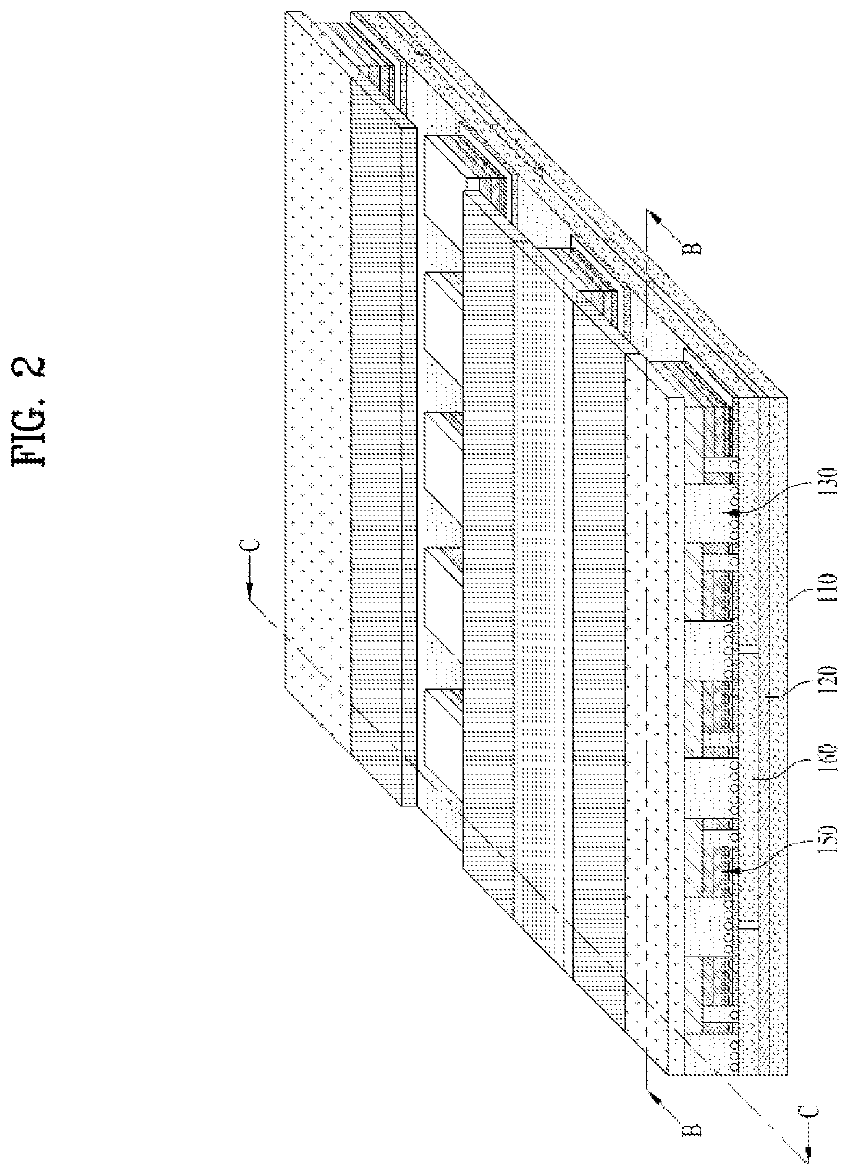
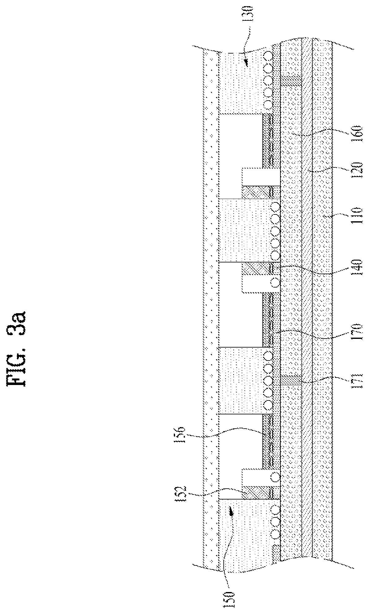
[0054]Reference will now be made in detail to embodiments of the present disclosure, examples of which are illustrated in the accompanying drawings. Wherever possible, the same reference numbers will be used throughout the drawings to refer to the same or like parts, and redundant description thereof will be omitted. As used herein, the suffixes “module” and “unit” are added or used interchangeably to facilitate preparation of this specification and are not intended to suggest distinct meanings or functions. In describing embodiments disclosed in this specification, relevant well-known technologies may not be described in detail in order not to obscure the subject matter of the embodiments disclosed in this specification. In addition, it should be noted that the accompanying drawings are only for easy understanding of the embodiments disclosed in the present specification, and should not be construed as limiting the technical spirit disclosed in the present specification.

[0...


PUM


Abstract

Disclosed in the present specification is a micro LED display device, and a manufacturing method therefor, the method forming, in advance, an anisotropic conductive adhesive paste layer only on a conductive electrode part of a semiconductor light emitting element and on a peripheral part thereof, and then transferring the anisotropic conductive adhesive paste layer to a wiring substrate, thereby simultaneously performing a transfer step and a stable wiring step.

Description

TECHNICAL FIELD[0001]The present disclosure relates to a display device and, more particularly, to a display device based on a micro light emitting diode (LED) and manufacturing method thereofBACKGROUND ART[0002]Recently, in a field of a display technology, display devices having excellent characteristics such as thinness, flexibility, and the like have been developed. On the other hand, currently commercialized major displays are represented by a LCD (liquid crystal display) and an OLED (organic light emitting diode).[0003]However, the LCD has a response time that is not fast, and is difficult to be flexibly implemented.[0004]On the other hand, LED (light emitting diode), which is a well-known semiconductor light-emitting element that converts electric current into light, has been used as a light source for a display image of an electronic device including an information and communication device along with a GaP:N-based green LED, starting with commercialization of a red LED using ...

Claims


Application Information

Patent Timeline
IPC IPC(8): H01L33/62H01L23/00H01L25/075H01L33/54H01L33/60
CPCH01L33/62H01L24/32H01L24/29H01L24/83H01L25/0753H01L33/54H01L33/60H01L2224/32227H01L2224/2949H01L2224/29386H01L2924/05341H01L2924/05442H01L2224/29499H01L33/0093H01L2933/0066H01L25/167H01L2933/0025H01L33/44H01L2224/95001H01L2224/1403H01L2224/83192H01L2924/18161H01L2224/8385H01L2224/73204H01L2924/0781H01L24/81H01L24/13H01L24/05H01L24/95H01L2224/16225H01L2224/2929H01L2924/12041H01L2224/83851H01L2224/83862H01L2224/32225H01L24/16H01L24/73H01L2224/16238H01L2224/83191H01L2224/83001H01L2224/294H01L2224/05599H01L2224/293H01L2224/13099H01L2224/83399H01L2924/00012H01L2924/00014H01L27/156H01L33/005H01L33/50H01L33/36H01L2224/1144H01L33/56H01L2224/29006H01L2224/32013H01L2224/83005H01L2224/83201H01L2224/95133
Inventor CHOI, HWANJOONWI, KYOUNGTAE
Owner LG ELECTRONICS INC
Why Eureka
Try Eureka