

Wafer transferring device
- Summary
- Abstract
- Description
- Claims
- Application Information
AI Technical Summary
Benefits of technology
Problems solved by technology
Method used
Image

Examples
Embodiment Construction
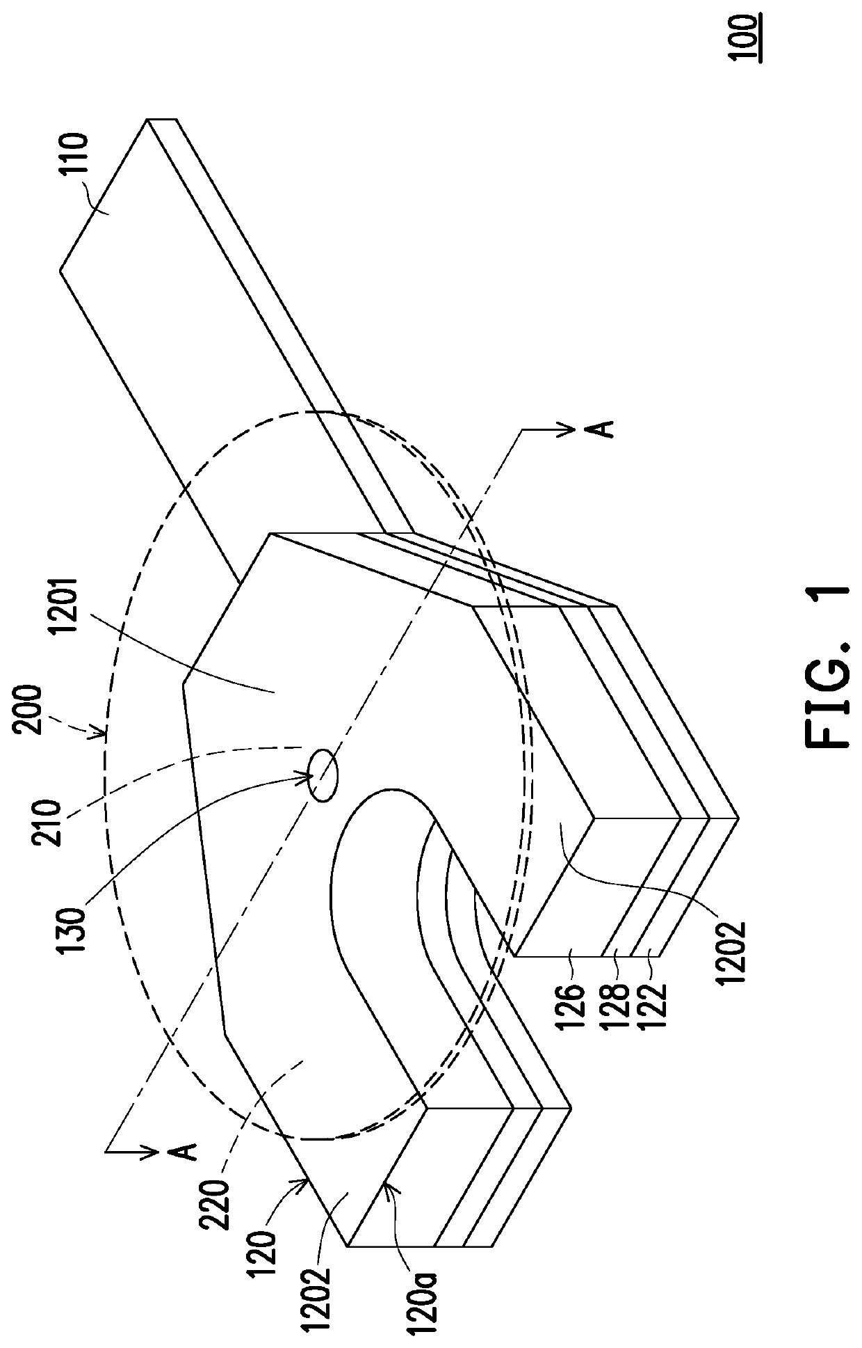
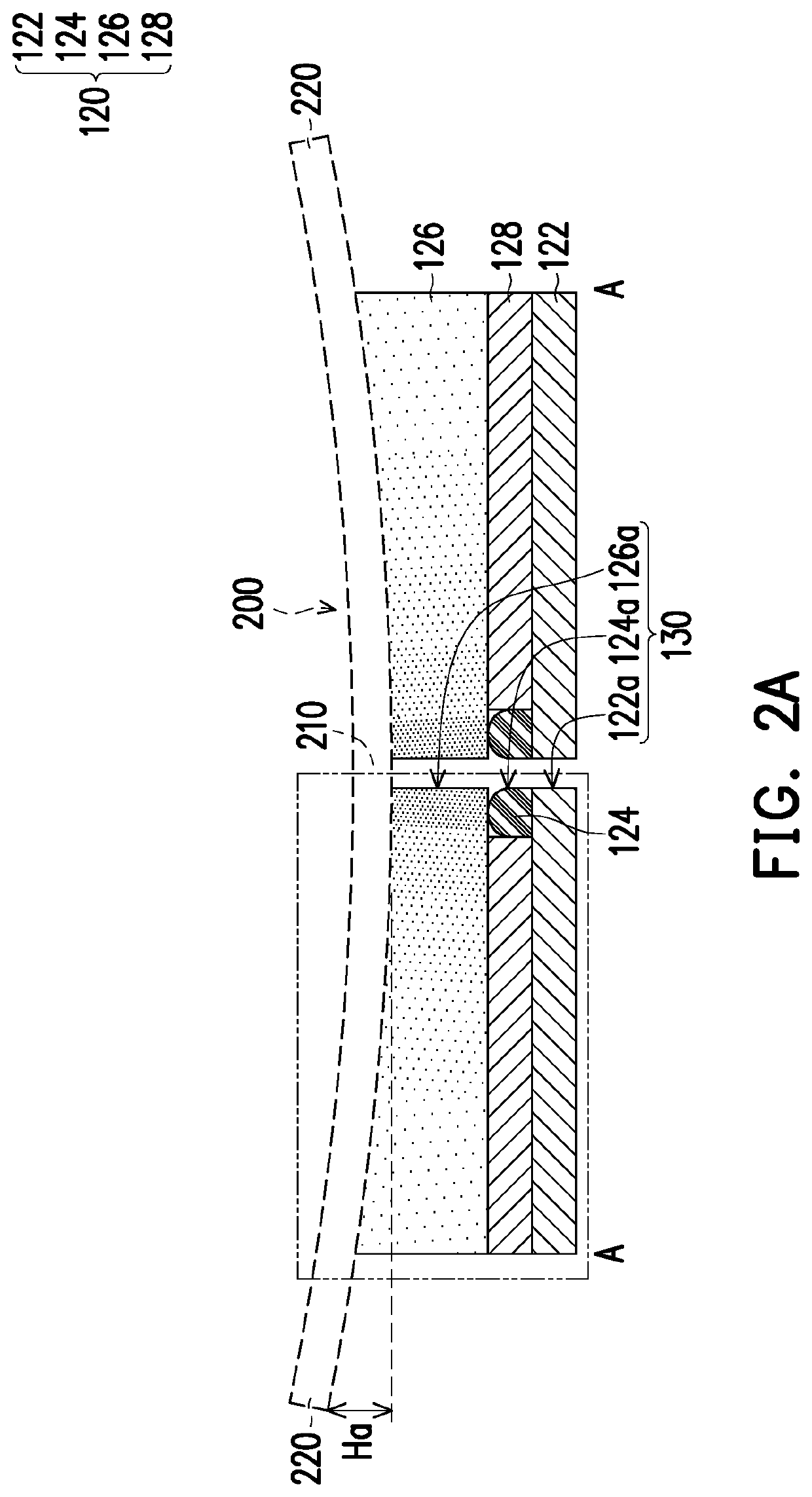
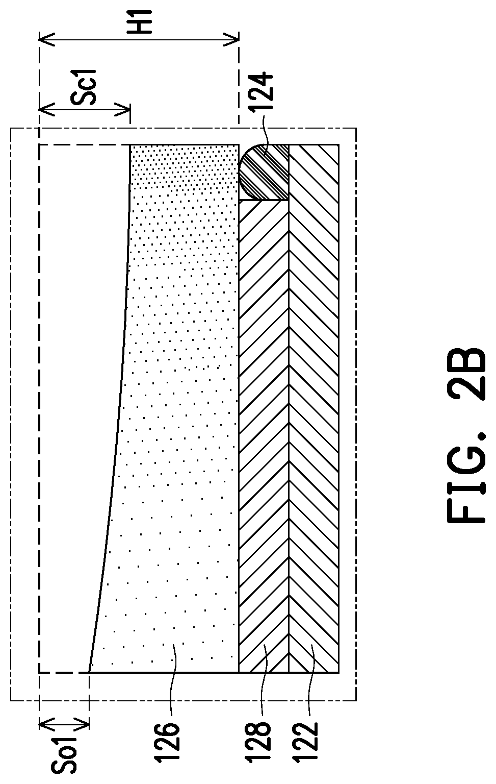
[0034]FIG. 1 is a schematic three-dimensional view of a wafer transferring device applied to a first wafer according to an embodiment of the invention. FIG. 2A is a schematic cross-sectional view of the wafer transferring device of FIG. 1 applied to the first wafer along a line A-A. Referring to FIG. 1 and FIG. 2A, the wafer transferring device 100 of the embodiment is adapted to suck and transfer a first wafer 200. It should be noted that the first wafer 200 in FIG. 1 and FIG. 2A is drawn with dashed lines in order to more clearly illustrate a structure of the wafer transferring device 100. In addition, proportional relationships of sizes and thicknesses between the wafer transferring device 100 and the first wafer 200 in the figures are only schematic.
[0035]Referring to FIG. 1, in the embodiment, the wafer transferring device 100 includes an arm 110 and a supporting carrier 120. The supporting carrier 120 is connected to the arm 110. The supporting carrier 120 has an upper surface...
PUM
 Abstract
Description
Claims
Application Information