Substrate transporting and processing system

a technology of transporting and processing system and substrate, which is applied in the direction of cleaning process and apparatus, cleaning using liquids, cleaning apparatus and processes, etc., and can solve the problems of reducing throughput, increasing the size of the whole system, and reducing the product yield

Inactive Publication Date: 2000-01-04
TOKYO ELECTRON LTD
View PDF17 Cites 76 Cited by
  • Summary
  • Abstract
  • Description
  • Claims
  • Application Information

AI Technical Summary

Problems solved by technology

However, since the size and weight of the wafers increase with the increase of the diameter of the wafers, if the vertically arranged wafers are transported from the supply section to the discharge section as the conventional manner, when the wafers are delivered between the supply and discharge sections and the processing section, there are problems in that the displacement of the wafers may occur and particles may be produced due to the movement of the wafers, so that the yield of products may be decreased.
In addition, with the increase of the diameter of the wafers, the size of the transport means and the respective processing units increases, so that there are problems in that the size of the whole system increases and the throughput decreases.
If the vapor leaks out of the cleaning system via the transport gate of the interface section, the interior of the clean room is contaminated.
If particles, together with the airflow, enter the interior of the cleaning system, or if the arrow in the s...

Method used


Image

  • Substrate transporting and processing system
  • Substrate transporting and processing system
  • Substrate transporting and processing system

Examples


Embodiment Construction

]

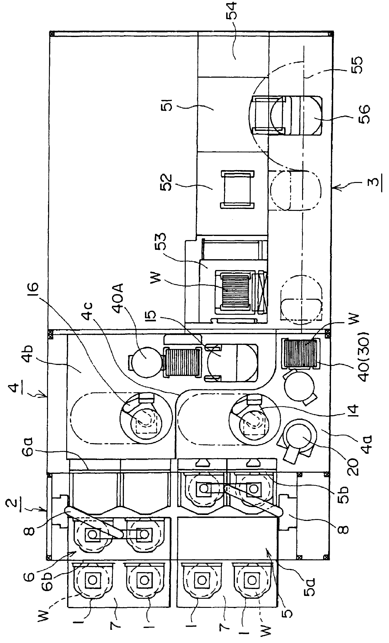
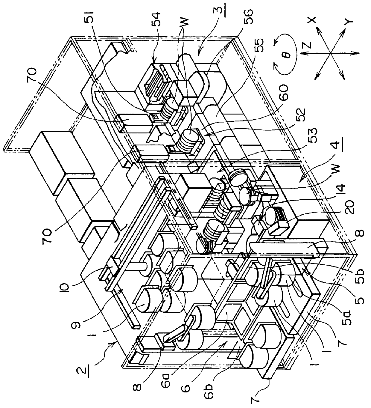
In the first preferred embodiment, while the wafer unloading arm 14 and the wafer loading arm 16 have been separately provided, e.g., two stages of wafer holding sections for holding the wafers W may be provided, so that the wafers W can be loaded into and unloaded from the carrier 1 by means of a single wafer loading / unloading arm having wafer loading and unloading portions. Therefore, since the wafers W can be loaded and unloaded by means of a single arm, the size of the system can be further decreased.

In the first preferred embodiment, while the wafer transport arm 56 for delivering the wafers W to the respective processing units of the processing section 3 and the wafer delivery arm 15 for receiving the processed wafers W have been provided, it is not always required to provide two kinds of arms, and a single transport arm may be used both as the wafer transport arm 56 and the wafer delivery arm 15.

In the preferred embodiments described above, while the substrate transporting a...


PUM


Abstract

A substrate transporting and processing system generally comprises: a supply section of a carrier 1 for housing therein wafers W to be processed, in a horizontal state; a discharge section of the carrier 1; a wafer unloading arm 14 for unloading the wafers W from said carrier 1; a wafer loading arm 16 for loading the wafers W into the carrier 1; an attitude changing unit 40 for changing the attitude of the wafers W between a horizontal state and a vertical state; a processing section 3 for suitably processing the wafers W; and a wafer transport arm 56 for delivering the wafers W between the attitude changing unit 40 and the processing section 3 and for transporting the wafers W into and from the processing section. Thus, after the wafers W housed in the carrier 1 in the horizontal state are unloaded and the attitude of the wafers W is changed into the vertical state, suitable processes are carried out, and the attitude of the wafers W is changed in the horizontal state after processing, so that the wafers W can be housed in the carrier 1. Thus, it is possible to decrease the size of the whole system to improve the throughput and to improve the yield of products.

Description

1. Field of the InventionThe present invention relates generally to a substrate transporting and processing system and a cleaning system. More specifically, the invention relates to a substrate transporting and processing system and cleaning system for sequentially transporting substrates to be processed, such as semiconductor wafers and glass substrates for LCDs, to suitably process the substrates.2. Description of the Prior ArtIn general, in production processes in semiconductor fabrication systems, substrate transporting and processing systems are widely used for sequentially transporting substrates to be processed, such as semiconductor wafers and glass substrates for LCDs (each of which will be hereinafter referred to as a "wafer"), to a processing bath for storing therein a processing solution, such as a chemical and a rinse solution (a cleaning solution), or a dying section to carry out the processings, such as cleaning and drying, of the wafers.In order to efficiently clean ...

Claims


Application Information

Patent Timeline
IPC IPC(8): H01L21/677H01L21/67H01L21/00
CPCH01L21/67173H01L21/67178H01L21/67757H01L21/67769H01L21/67775H01L21/67778Y10S134/902H01L21/68
Inventor KANEKO, SATOSHIKAMIKAWA, YUJIKOGUCHI, AKIRAKURODA, OSAMUKITAHARA, SHIGENORINISHIDA, TATSUYA
Owner TOKYO ELECTRON LTD
Why Eureka
Try Eureka