Method of optically inspecting multi-layered electronic parts and the like with fluorescent scattering top layer discrimination and apparatus therefor

a multi-layer electronic and top layer technology, applied in the field of optical inspection of multi-layered electronic parts and the like with fluorescent scattering top layer discrimination and apparatus therefor, can solve the problems of not being able to discriminate shallow angle illumination, color discrimination, etc., and not being able to properly optically image for defects. , to achieve the effect of detecting the top conductor pattern image by using dark fields

Inactive Publication Date: 2000-01-11
BELTRONICS
View PDF4 Cites 57 Cited by
  • Summary
  • Abstract
  • Description
  • Claims
  • Application Information

AI Technical Summary

Benefits of technology

The primary object of the present invention, accordingly, is to provide a new and improved method of and apparatus for enabling the discriminating and selective optical inspection of defects and the like of top layers of a multi-layered electronic part and the like comprising also intermediate and bottom layers, wherein the top layer includes a pattern of conductors, such as lines and the like to be dis

Problems solved by technology

The conductors are generally metal that can have a very rough finish, such as copper, oxidized copper, reflowed copper with a tin covering and the like, wherein the rough surfaces prove to difficult properly optically image to inspect for defects.
This problem resides from the compounding of reflections from all the superposed layers since the reflected incident light reflects from the

Method used


Image

  • Method of optically inspecting multi-layered electronic parts and the like with fluorescent scattering top layer discrimination and apparatus therefor
  • Method of optically inspecting multi-layered electronic parts and the like with fluorescent scattering top layer discrimination and apparatus therefor
  • Method of optically inspecting multi-layered electronic parts and the like with fluorescent scattering top layer discrimination and apparatus therefor

Examples


Embodiment Construction

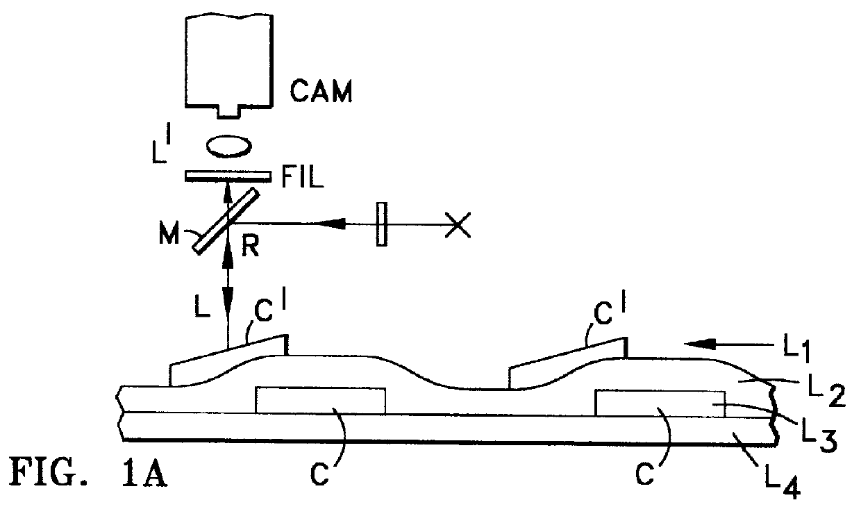
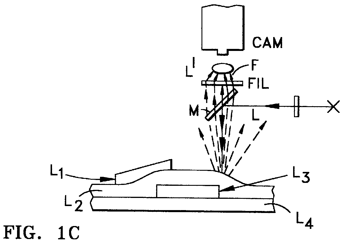
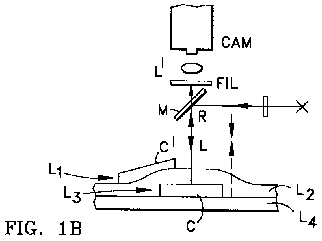
A typical multi-layer chip of the character above-described is shown in FIGS. 1A-C, comprising a base or substrate layer L.sub.4 as of ceramic, for example, shown carrying a layer L.sub.3 of metal conductors C thereupon, and in turn covered by an intermediate layer L.sub.2, generally preferably translucent or transparent as, for example, of organic polyimid material and the like, which insulates the lower layer conductors C from further conductors C.sup.1 on a top layer L.sub.1 superposed upon the intermediate insulating layer L.sub.2.

Incident light L from a light source is illustrated as directed by a half-silvered mirror M upon the top layer L.sub.1 of the chip and reflects from the top layer pattern of conductors C.sup.1. The solid vertical arrowed lines indicate light-illuminating incidence L and reflection R back towards the inspection camera CAM. Since the intermediate insulation layer L.sub.2 covering the lower conductors C of the layer L.sub.3 will not be flat but irregular ...


PUM


Abstract

A novel optical inspection technique for multi-layer wafers and the like in which conductor patterns of a top layer only are to be inspected, such layer being upon an intermediate transparent or translucent insulation layer in turn upon a base layer(s) thereunder, wherein the intermediate layer only is fluoresced, displaying the top layer conductors as dark in the field of fluorescent light, and causing reflections from layers below the intermediate layer effectively to disappear to obviate confusion with the top layer conductors to be inspected.

Description

The present invention relates to the optical inspection of electronic parts and the like, being more particularly directed to multi-layered electronic parts such as those used for wafers from which integrated circuit chips are formed, flat display panels, multi-chip modules, and flexible circuit patches and decals, etc., wherein there are top layers of conductors in various patterns, an intermediate layer (sometimes externally carrying the conductor layer on top) and comprising transparent or translucent insulation, and base substrate or bottom layers as of ceramic, glass, metal and the like, also often carrying conductors in various patterns.Fluorescent light emissions have previously been used to inspect electronic circuit boards consisting of layers of epoxy containing conductors defining circuits deposited therein. The conductors are generally metal that can have a very rough finish, such as copper, oxidized copper, reflowed copper with a tin covering and the like, wherein the r...

Claims


Application Information

Patent Timeline
IPC IPC(8): G01N21/95G01N21/88
CPCG01N21/9501G01N21/956
Inventor BISHOP, ROBERT
Owner BELTRONICS
Why Eureka
Try Eureka