Small amplitude signal output circuit
a small amplitude signal and output circuit technology, applied in logic circuit coupling/interface arrangement, pulse technique, instruments, etc., can solve the problems of reducing and canceling the advantages of the small amplitude transmission described before, the variation of output signal amplitude is considerably large, and the power source potential supplied from outside the integrated circuit changes
- Summary
- Abstract
- Description
- Claims
- Application Information
AI Technical Summary
Problems solved by technology
Method used
Image

Examples
first embodiment
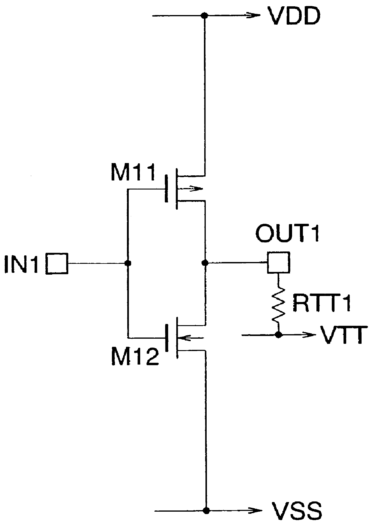
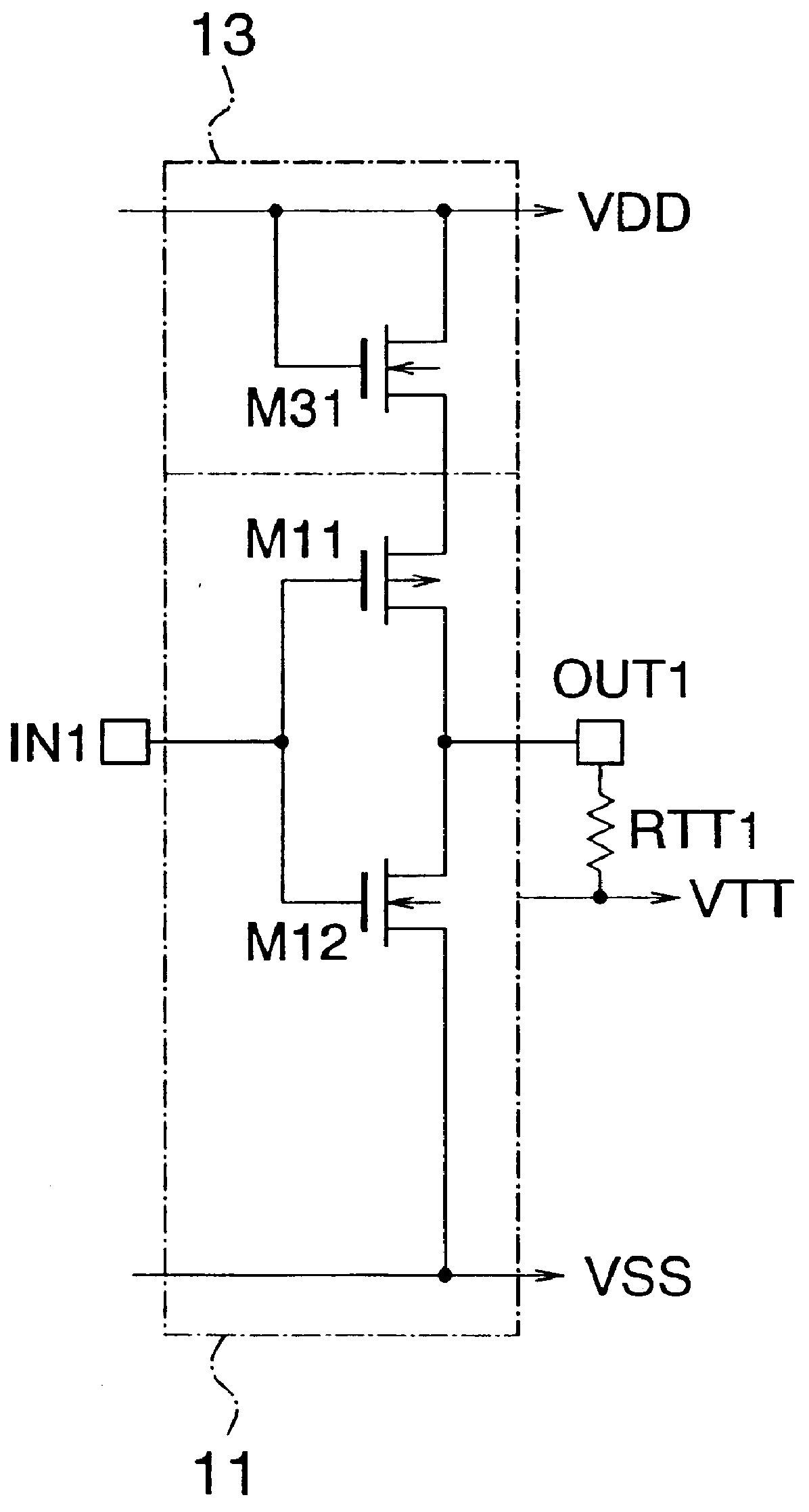
Referring to FIG. 3 showing a circuit diagram of an output circuit according to the present invention, the output circuit comprises an output section 11 having pMOS transistor M11 and nMOS M12, a terminal resistor RTT1, an input terminal IN1 and an output terminal OUT1, which are similar to those in the first conventional output circuit. In addition, the output circuit comprises a voltage control section 13, connected between a power source line VDD and the source of transistor M11, for controlling the voltage level of transistor M11.
Voltage control section 13 comprises an nMOS transistor M31 having a gate and a drain connected together to power source line VDD and a source connected to the source of the transistor M31 of output circuit 11, thereby forming a diode structure.
In operation, when a signal potential at L-level which is close to the potential of power source voltage VSS is supplied to input terminal IN1 and transistor M11 of output circuit 11 is ON, transistor M12 is OFF,...
fourth embodiment
In the above embodiments, gate-source voltage of a nMOS / pMOS transistor forming a diode structure or diode connection is used in the voltage control section. Base-emitter voltage of nMOS / pMOS transistor forming a diode connection may also be used instead. The gate-source voltage or the base-emitter voltage, however, varies with the temperature change. Generally, higher temperature results in a lower gate-source voltage or lower base-collector voltage. That is, L-level VOH and H-level VOL of output signals vary according to expressions (9) and (12). the present invention described hereinafter can be used to suppress the voltage change caused by a temperature fluctuation.
Referring to FIG. 6, the output circuit according to the present embodiment is similar to the first embodiment except that a voltage control section 15 is provided in the present embodiment instead of voltage control section 13 of the first embodiment.
Voltage control section 15 comprises: a PNP transistor M51 having a...
fifth embodiment
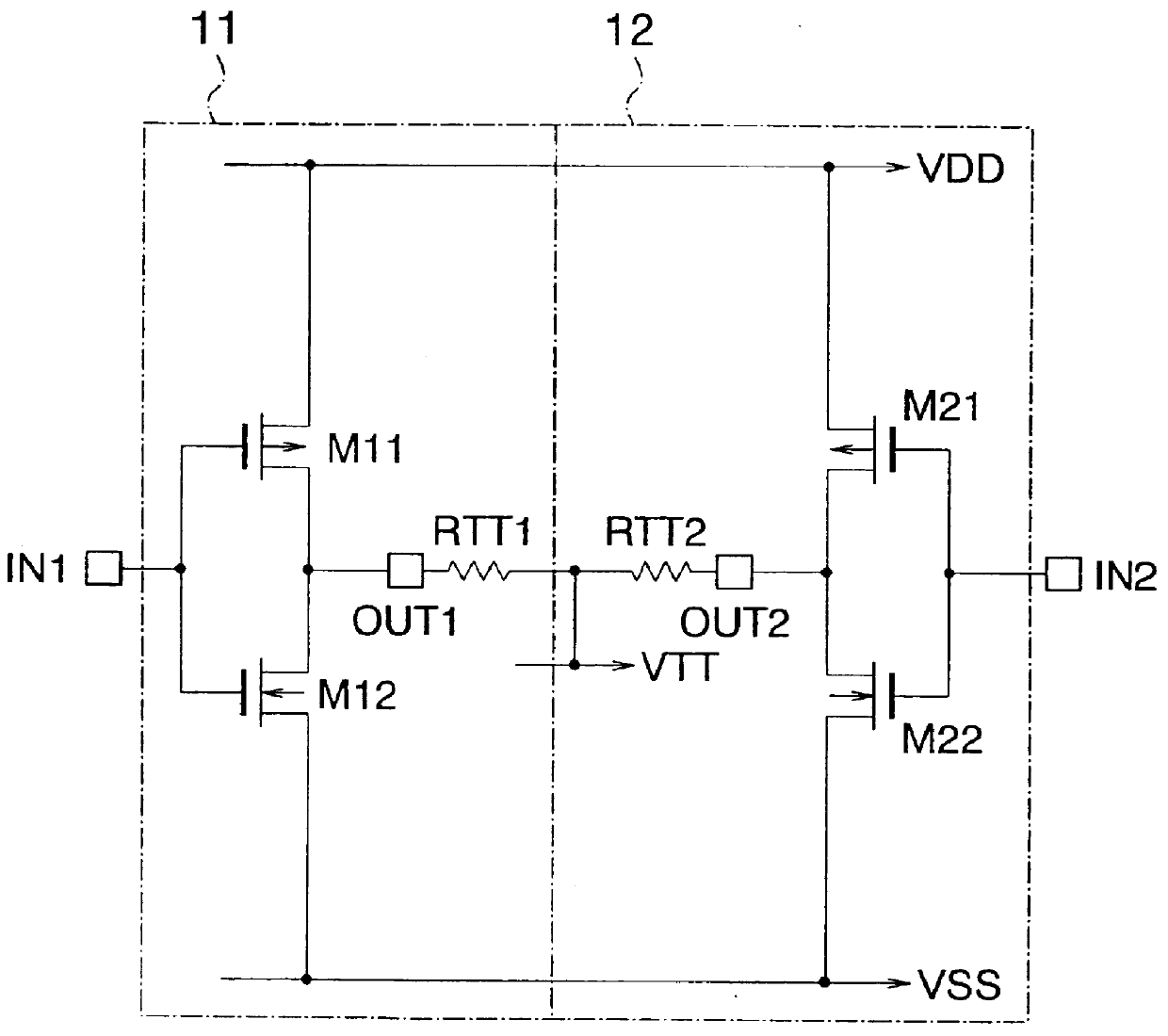
Since the present embodiment is directed to the differential transmission system, there exist two input terminals 1N1 and IN2 and two output terminals OUT1 and OUT2. However, it will be understood that the output section 11 and the voltage control section 16A are similar to those in the fifth embodiment directed to a single phase transmission system. The same applies to output section 12.
Output sections 11 and 12 and voltage control section 16A of the present embodiment operate similarly to those in the fifth embodiment. Accordingly, descriptions of the operation is omitted herein for avoidance of duplication.
In the present embodiment, a single voltage control section 16A is provided for the pair of output sections 11 and 12. A pair of voltage control sections 16A may be provided, although the operation and the advantages are little improved from the single voltage control section.
In the above embodiments, the first to fifth embodiments are directed to the single phase transmission ...
PUM
 Abstract
Description
Claims
Application Information
 - R&D Engineer
- R&D Manager
- IP Professional
- Industry Leading Data Capabilities
- Powerful AI technology
- Patent DNA Extraction
Browse by: Latest US Patents, China's latest patents, Technical Efficacy Thesaurus, Application Domain, Technology Topic.
© 2024 PatSnap. All rights reserved.Legal|Privacy policy|Modern Slavery Act Transparency Statement|Sitemap