Memory cell having a reduced active area and a memory array incorporating the same

a memory cell and active area technology, applied in the field of memory cells, can solve the problem of less than optimal repeatability

Inactive Publication Date: 2000-07-11
ROUND ROCK RES LLC
View PDF52 Cites 36 Cited by
  • Summary
  • Abstract
  • Description
  • Claims
  • Application Information

AI Technical Summary

Problems solved by technology

All of these methods suffer from technological constraints upon the

Method used


Image

  • Memory cell having a reduced active area and a memory array incorporating the same
  • Memory cell having a reduced active area and a memory array incorporating the same
  • Memory cell having a reduced active area and a memory array incorporating the same

Examples


Embodiment Construction

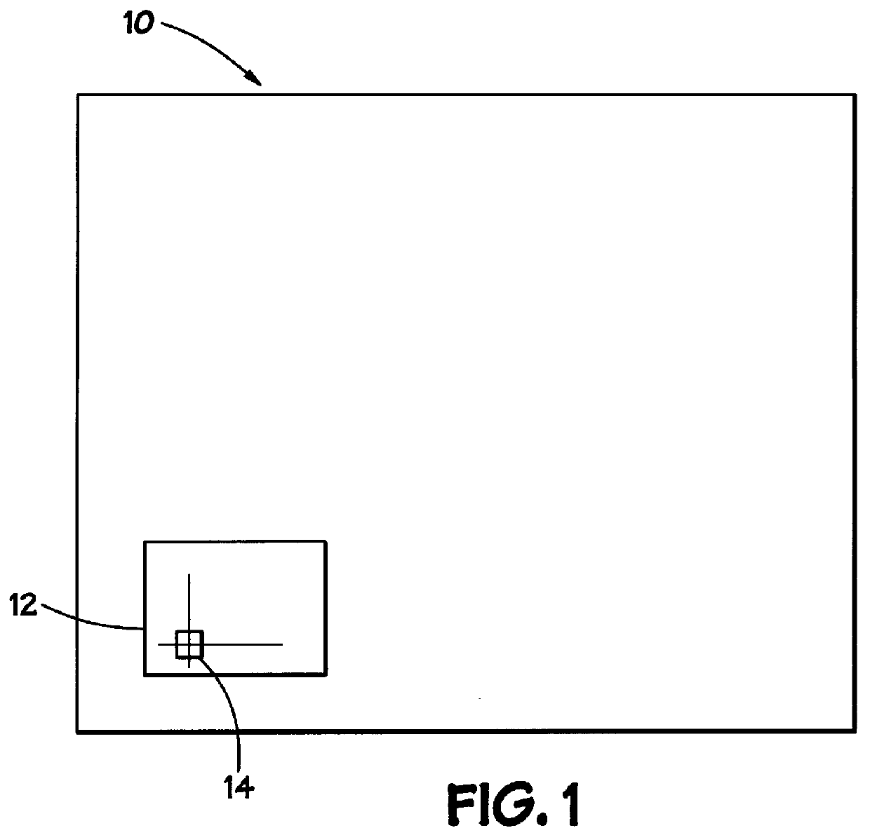
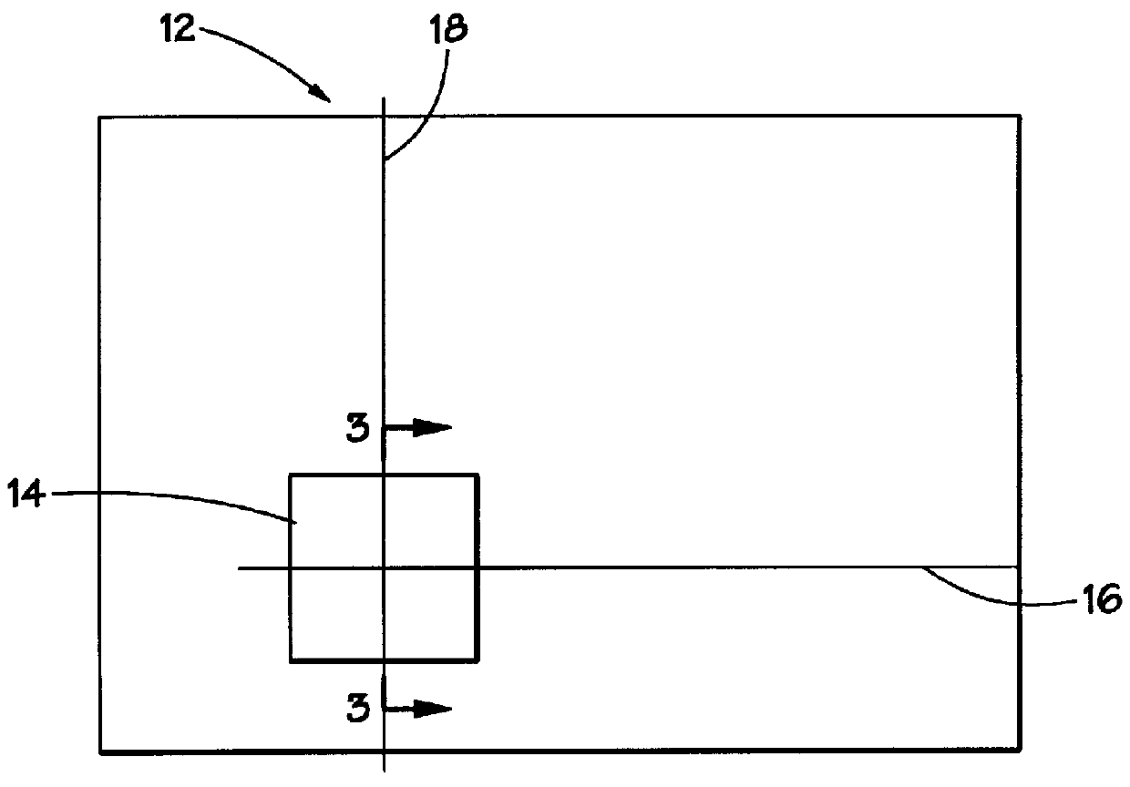
Turning now to the drawings, and referring initially to FIG. 1, a memory device is illustrated and generally designated by a reference numeral 10. The memory device 10 includes a plurality of memory arrays 12, one of which is illustrated. Each memory array 12 includes a plurality of memory cells 14, one of which is illustrated in FIG. 2. The memory cells 14 are arranged in rows and columns. Memory cells 14 in each row are connected by a respective row line 16, and memory cells 14 in each column are connected by a respective column line 18. Each memory cell 14 can be accessed for reading or writing by selecting the corresponding row and column coordinates and applying the appropriate voltage or current signal.

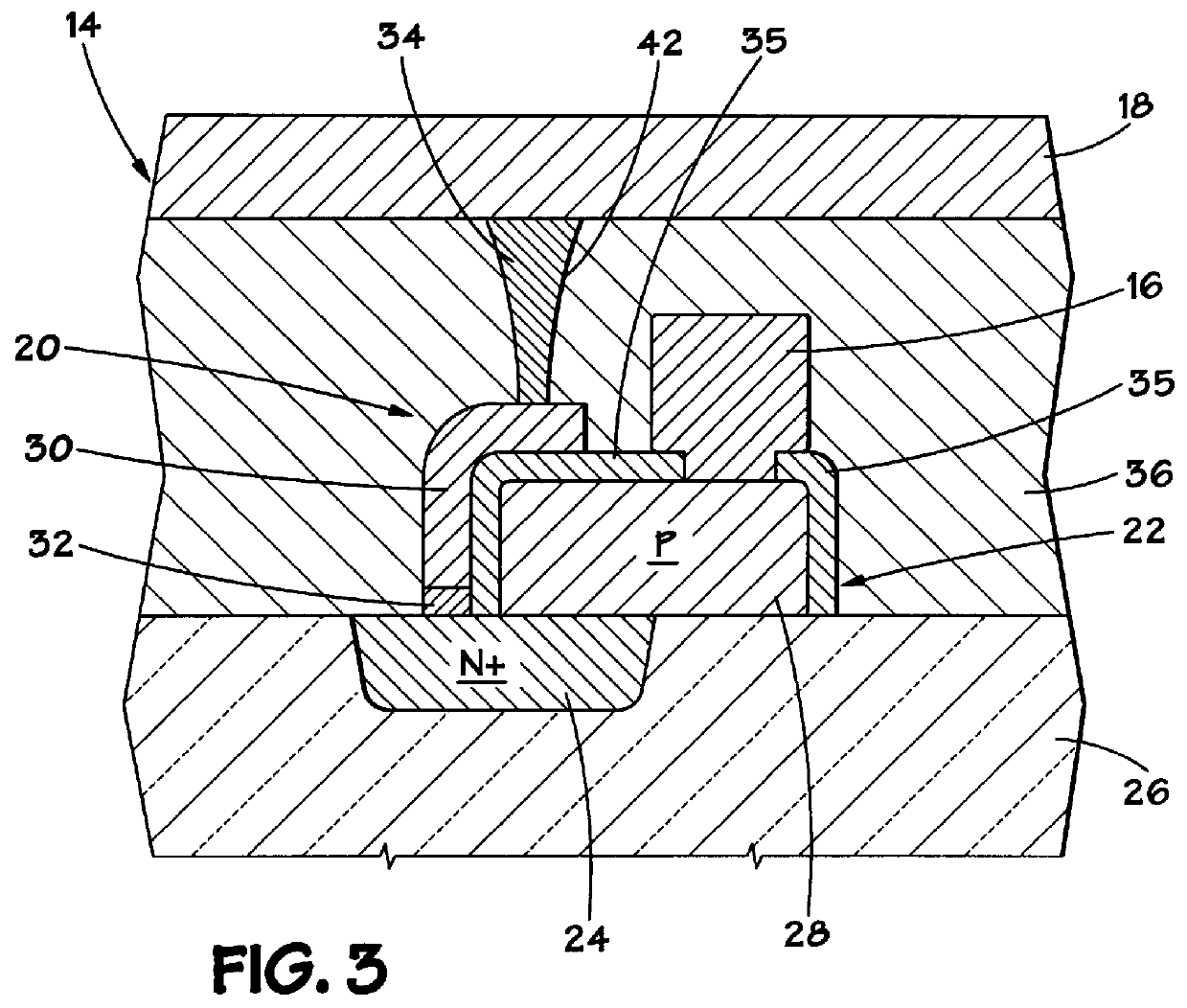
FIG. 3 illustrates an exemplary memory cell 14. The memory cell 14 includes a memory element 20 coupled to an access device 22. The memory element 20 and the access device 22 are coupled between a respective row line 16 and a respective column line 18. The access device 22 is a ...


PUM


Abstract

There is disclosed a memory cell having a reduced active area. The memory cell may be incoporated into a memory array. A method of fabricating the memory cell and the memory array includes the fabrication of an access device, such as a diode, that protrudes above the semiconductor substrate. The memory element, such as a memory element formed of chalcogenide material, is disposed on the side of the protrusion to reduce the active area of the memory element as compared with conventional memory elements.

Description

1. Field of the InventionThe present invention relates generally to the manufacture of semiconductor memory devices and, more particularly, to the formation of memory cells having active areas of reduced cross-sectional size.2. Background of the Related ArtMemory devices are integrated circuits that store information, typically for use by a microprocessor. A memory device can have a plurality of memory arrays, and each memory array can include hundreds of thousands of memory cells. Each memory cell generally includes a memory element and an access device coupled to the memory element. The memory cell may store information by storing a charge or by changing resistivity.Chalcogenide materials recently have been proposed to form memory elements in memory devices. Chalcogenides are materials which may be electrically stimulated to change states, from an amorphous state to a crystalline state, for example, or to exhibit different resistivities while in the crystalline state. Thus, chalco...

Claims


Application Information

Patent Timeline
IPC IPC(8): H01L29/66H01L27/102H01L27/24H01L29/861H01L45/00
CPCH01L27/1021H01L29/8615H01L45/06H01L27/2463H01L45/144H01L45/1691H01L27/2409H01L45/124H10B63/20H10B63/80H10N70/8265H10N70/231H10N70/8828H10N70/068
Inventor REINBERG, ALAN R.
Owner ROUND ROCK RES LLC
Why Eureka
Try Eureka