Flash memory and program verify method for flash memory

a flash memory and program verification technology, applied in the field of flash memory, can solve problems such as reliability reduction, and achieve the effect of high reliability

Active Publication Date: 2007-12-25
TOWER SEMICONDUCTOR +1
View PDF10 Cites 18 Cited by
  • Summary
  • Abstract
  • Description
  • Claims
  • Application Information

AI Technical Summary

Benefits of technology

[0015]Therefore, an object of the present invention is to provide a flash memory which eliminates an influence of the neighbor cell effect and has a high level of reliability, and a program verify method for the same.

Problems solved by technology

However, a flash memory having the virtual ground array type memory array has a problem that a neighbor cell effect occurs in the memory array, resulting in a reduction in reliability.

Method used


Image

  • Flash memory and program verify method for flash memory
  • Flash memory and program verify method for flash memory
  • Flash memory and program verify method for flash memory

Examples


Embodiment Construction

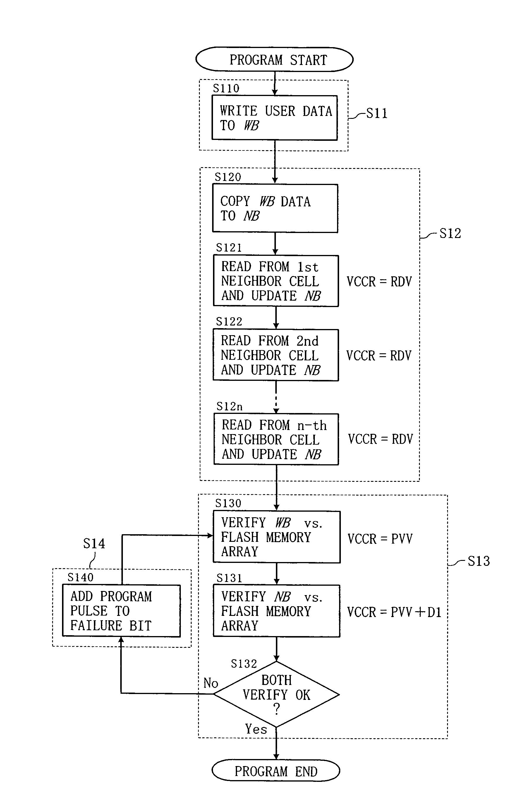
[0056]Hereinafter, a flash memory and a program verify method thereof according to an embodiment of the present invention will be described with reference to the accompanying drawings. Particularly, a hardware structure, a neighbor cell effect and measures thereagainst, structures of a write buffer and a neighbor cell buffer, an offset addition process, a first program verify process, and a second program verify process, will be described in this order.

[0057](Hardware Structure)

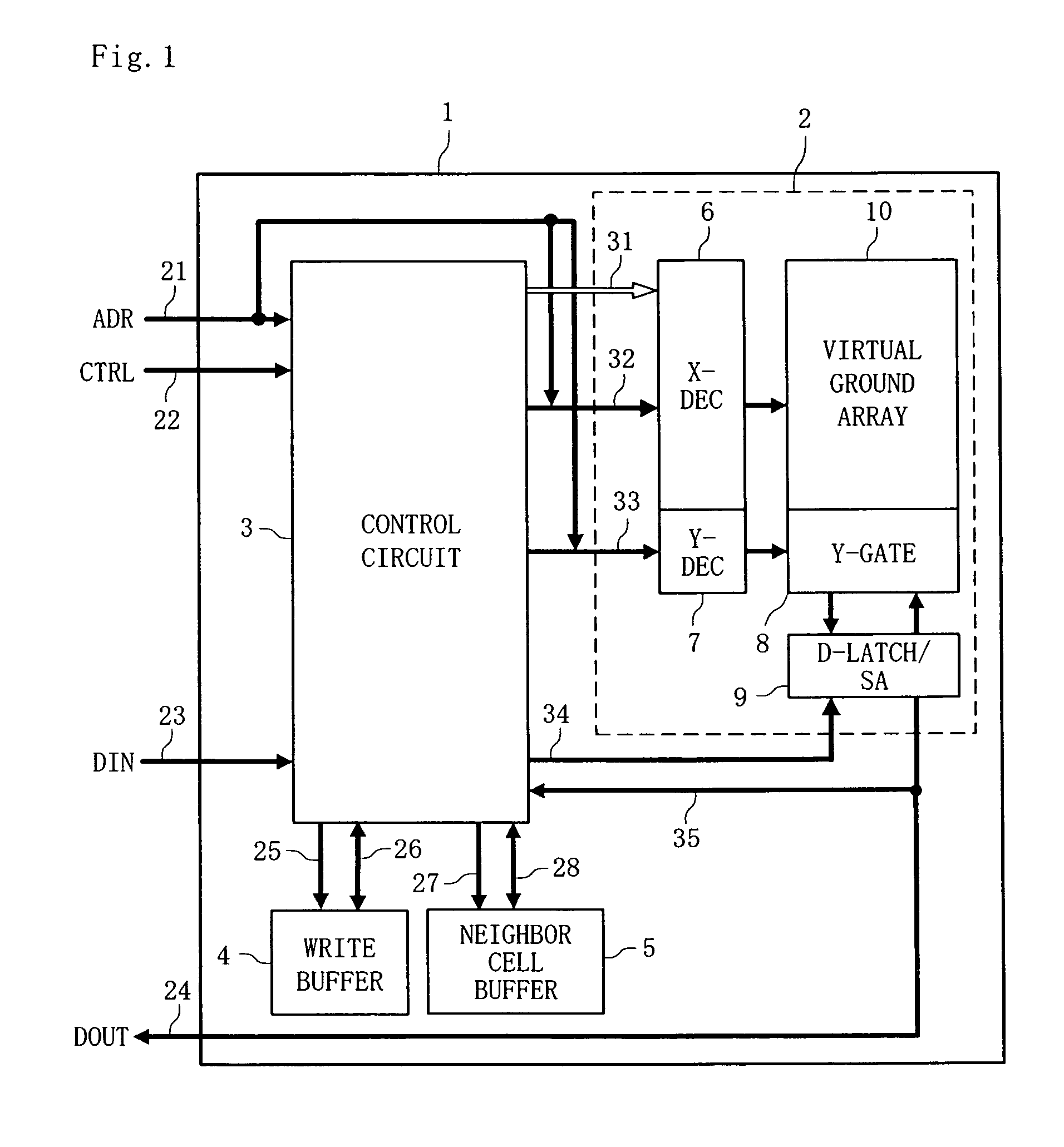
[0058]FIG. 1 is a block diagram of a flash memory according to an embodiment of the present invention. The flash memory 1 of FIG. 1 comprises a flash memory array 2, a control circuit 3, a write buffer 4, and a neighbor cell buffer 5. The flash memory array 2 includes an X decoder 6, a Y decoder 7, a Y gate 8, a data latch / sense amplifier 9, and a virtual ground array 10.

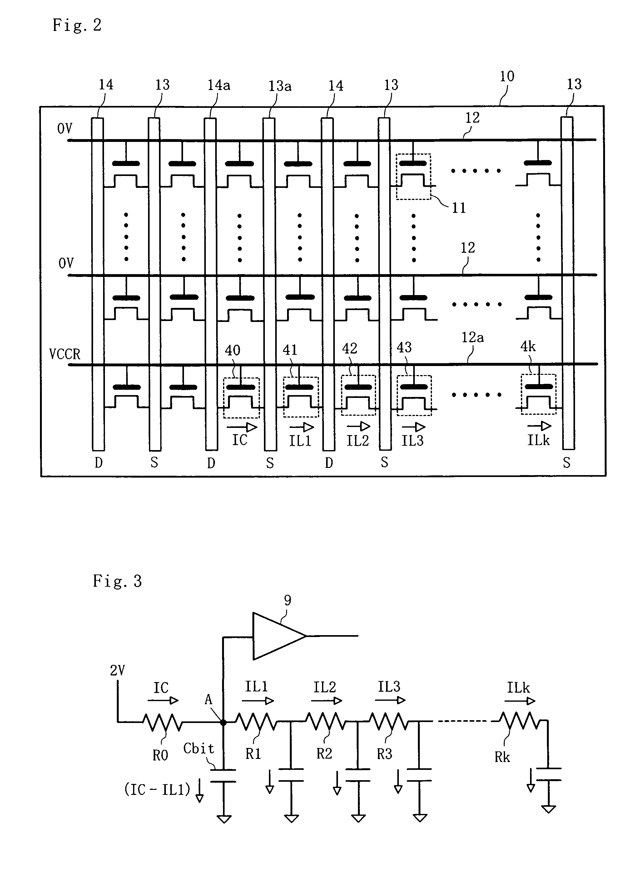
[0059]The virtual ground array 10 includes memory cells, word lines and bit lines which are arranged in a two-dimensional manner (described ...


PUM


Abstract

In conventional memory arrays in which a bit line is shared by memory cells, a cell current flows over into neighbor cell(s) in a program verify process, and therefore, the threshold of a memory cell to be programmed is erroneously determined to be lower. Therefore, in a program verify process, a control circuit 3 writes a fail value to a neighbor cell buffer 5 when all neighbor cell(s) having an offset of n or less from a memory cell to be programmed are in the erased state, and when otherwise, writes a pass value to the neighbor cell buffer 5. The control circuit 3 verifies input write data and also verifies data stored in the neighbor cell buffer(s). In the latter verify process, a verify voltage higher than an ordinary one is used to compensate for the leakage of cell current.

Description

BACKGROUND OF THE INVENTION[0001]1. Field of the Invention[0002]The present invention relates to a flash memory comprising a memory array in which a bit line is shared by memory cells, and a program verify method for the same.[0003]2. Description of the Background Art[0004]In conventional non-volatile memories, such as a flash memory, an EEPROM and the like, a floating gate type memory cell which uses an electrical conductor material (e.g., polysilicon, etc.) as data storage means is employed. In recent years, an NROM (Nitride Read-Only Memory) type memory cell which uses an insulator ONO film (a composite structure of a nitride film and oxide films) has attracted attention as data storage means in order to improve the degree of integration and reliability.[0005]When the NROM type memory cell is used to construct a memory array, a virtual ground array technology is employed in which a bit line is shared by memory cells neighboring each other. In the virtual ground array type memory ...

Claims


Application Information

Patent Timeline
Patent Type & Authority Patents(United States)
IPC IPC(8): G06F12/00G11C11/34G11C16/34
CPCG11C16/3454
Inventor TOMITA, YASUHIROSUWA, HITOSHIKOMIYA, MANABUTOTH, TAMASJACOB, JEFFREY ALLANPARVIN, AVIESHEL, NOAM
Owner TOWER SEMICONDUCTOR
Why Eureka
Try Eureka