Nonvolatile semiconductor memory device

a semiconductor memory and non-volatile technology, applied in static storage, digital storage, instruments, etc., can solve the problems of increasing the proportion of circuits in the chip, the eeproms of floating gate type approaching their limit, and the eeproms of floating gate type becoming more and more complicated

Active Publication Date: 2010-12-23
KIOXIA CORP
View PDF2 Cites 21 Cited by
  • Summary
  • Abstract
  • Description
  • Claims
  • Application Information

AI Technical Summary

Problems solved by technology

However, the miniaturization of the EEPROMs of the floating gate type is approaching its limit these days.
To further improve the protection performance for confidential data, the circuit becomes more and more complicated, and the proportion of the circuit in the chip becomes larger.

Method used


Image

  • Nonvolatile semiconductor memory device
  • Nonvolatile semiconductor memory device
  • Nonvolatile semiconductor memory device

Examples


first embodiment

[0030][Entire Structure of Nonvolatile Semiconductor Memory Device according to First Embodiment]

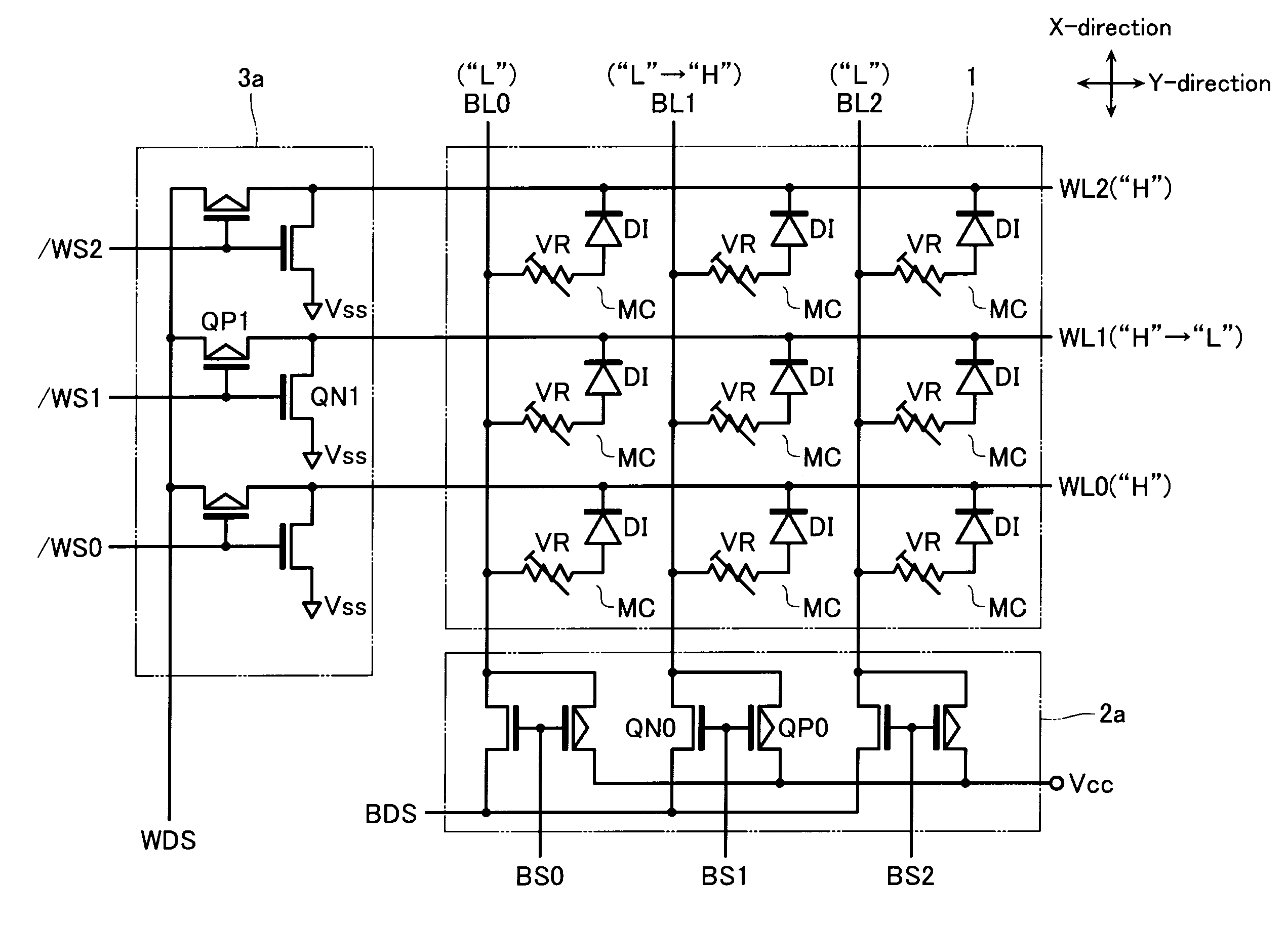
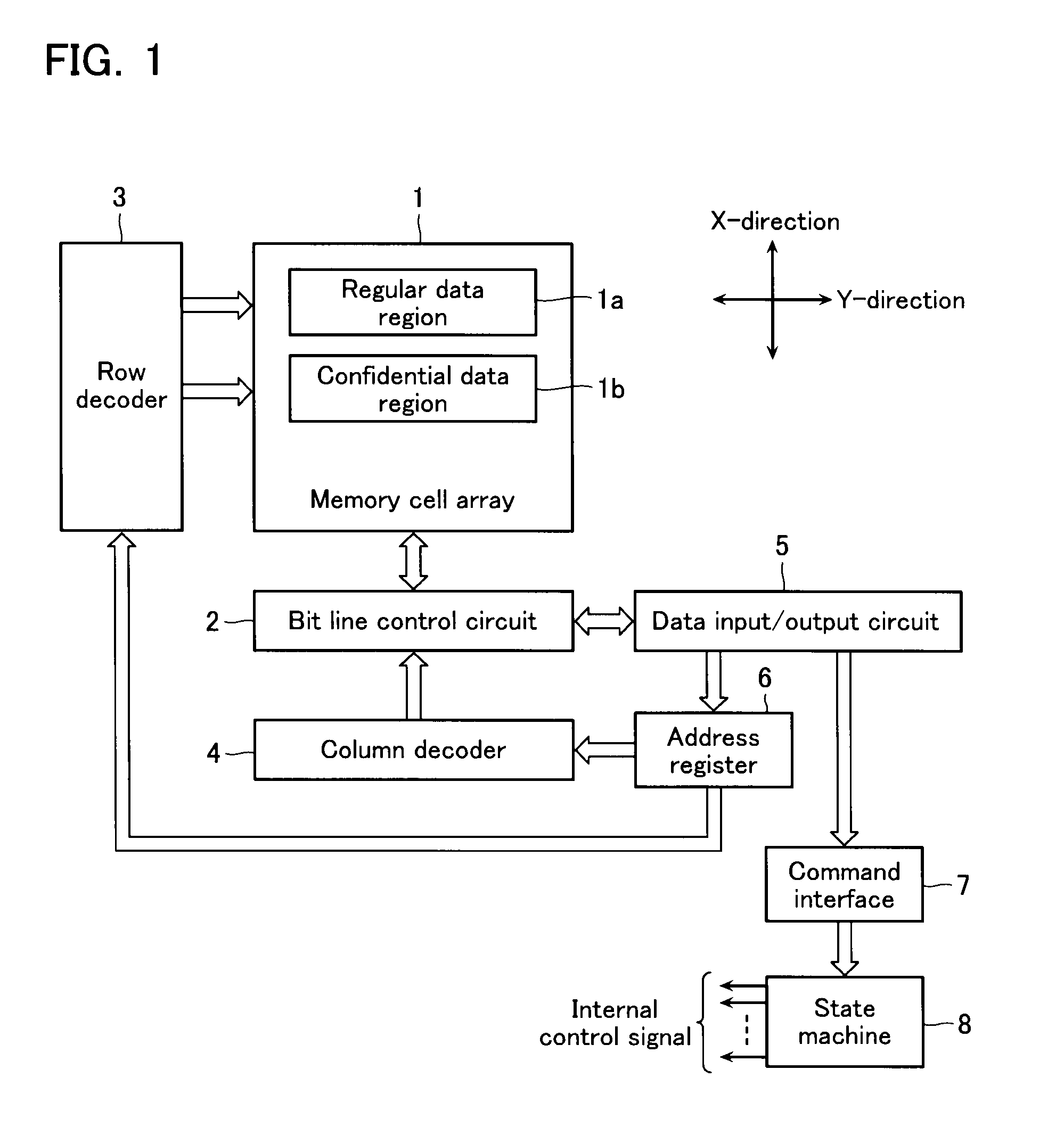
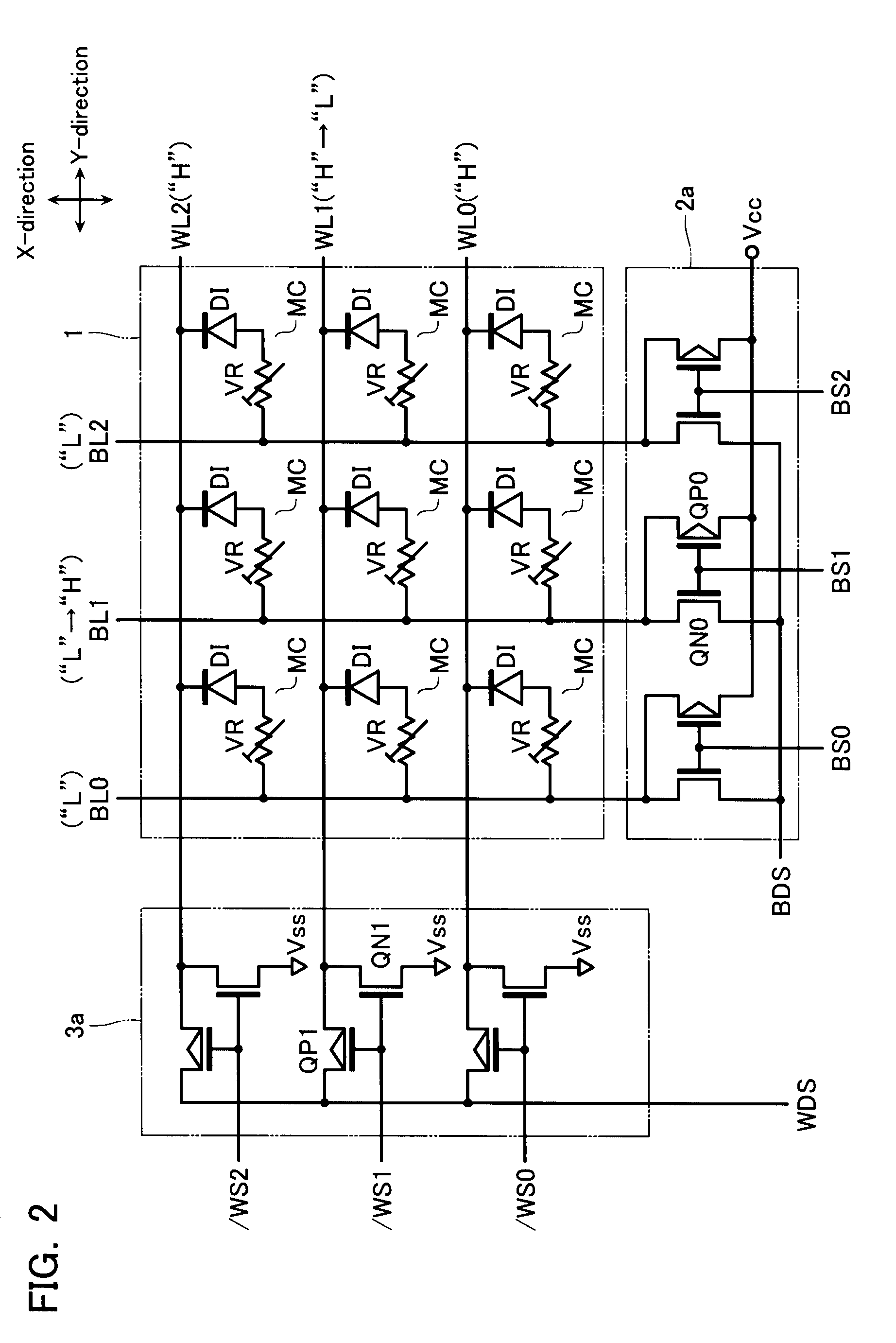
[0031]Referring to FIG. 1, the entire structure of a nonvolatile semiconductor memory device according to an embodiment of the present invention is first described. In the first embodiment, the nonvolatile semiconductor memory device is described as a resistive memory device that includes variable resistive elements VR as memory cells MC as described later. FIG. 1 is a block diagram of the nonvolatile semiconductor memory device according to this embodiment of the present invention. The nonvolatile semiconductor memory device according to this embodiment includes a memory cell array 1 and peripheral circuits as a control circuit that performs control operations such as data rewriting, holding, and reading.

[0032]The memory cell array 1 includes a regular data region 1a and a confidential data region 1b. Although the regular data region 1a and the confidential data region 1b are provided i...

second embodiment

[0089][Structure of Nonvolatile Semiconductor Memory Device according to Second Embodiment]

[0090]Next, a nonvolatile semiconductor memory device according to a second embodiment of the present invention is described. The nonvolatile semiconductor memory device according to this embodiment differs from that according to the first embodiment in being a NAND-type EEPROM including memory cells MC that each change the threshold voltage by injecting and releasing electrons into a floating gate.

[0091]FIG. 10 is a circuit diagram of a memory cell array 1 and its peripheral circuits. The memory cell array 1 of the nonvolatile semiconductor memory device of this embodiment is formed by arranging nonvolatile memory cells MC in a matrix fashion, as shown in FIG. 10. The nonvolatile memory cells MC can be electrically rewritten. Each of the memory cells MC includes an n-type source / drain diffusion layer formed on p-well of a silicon substrate, and is a stack gate structure including a floating g...


PUM


Abstract

According to one embodiment, a nonvolatile semiconductor memory device includes a memory cell array including regular memory cells and permanent memory cells and a control circuit. The regular memory cells are capable of switching between a first data storage state and a second data storage state. The permanent memory cells are fixed in a third data storage state that is read as the same logic level data as the first storage state. Data is stored in at least one of the regular memory cells and at least one of the permanent memory cells. The control circuit rewrites at least one of the regular memory cells from the second data storage state to the first data storage state at the time of data holding. The control circuit performs a reading operation after rewriting the regular memory cells from the first data storage state to the second data storage state.

Description

CROSS REFERENCE TO RELATED APPLICATIONS[0001]This application is based upon and claims the benefit of priority from the prior Japanese Patent Application No. 2009-144984, filed on Jun. 18, 2009, the entire contents of which are incorporated herein by reference.BACKGROUND[0002]1. Field[0003]Embodiments described herein relate generally to a nonvolatile semiconductor memory device.[0004]2. Description of the Related Art[0005]As one of the electrically-rewritable nonvolatile semiconductor memories (EEPROMs), a NAND-type EEPROM that can be highly integrated is well known. In the NAND-type EEPROM, data rewriting is normally performed by injecting electrons into and releasing electrons from a floating gate via an oxide film much thinner than the gate oxide film that is used in a conventional MOSFET. Higher-density EEPROMs have been realized through miniaturization achieved by the advanced processing technology and device technology. However, the miniaturization of the EEPROMs of the float...

Claims


Application Information

Patent Timeline
Patent Type & Authority Applications(United States)
IPC IPC(8): G11C16/04G11C11/00G11C7/00
CPCG11C13/0069G11C2213/72G11C17/165G11C17/16G11C11/005G11C13/0059
Inventor YONEYA, KAZUHIDETSUCHIYA, KENJI
Owner KIOXIA CORP
Why Eureka
Try Eureka