Data latch circuit

a data latch and circuit technology, applied in the field of data latch circuits, can solve the problems of increasing the the transmission of an error signal, and the general difficulty in determining the optimum timing of the data latch

Inactive Publication Date: 2000-08-08
RENESAS ELECTRONICS CORP
View PDF7 Cites 6 Cited by
  • Summary
  • Abstract
  • Description
  • Claims
  • Application Information

AI Technical Summary

Problems solved by technology

If the data is latched at the timing at which the amplitudes of data waveforms 22 and 23 shown in FIG. 2 are small, the latch section cannot correctly determine the data, resulting in transmission of an error signal.
Particularly, in the case of a high-speed semiconductor device, since the time length of period T2 therein is short, the optimum timing of the data latch is generally diff

Method used


Image

  • Data latch circuit
  • Data latch circuit
  • Data latch circuit

Examples


Embodiment Construction

Now, the present invention is more specifically described with reference to accompanying drawings, wherein similar constituent elements are designated by similar reference numerals throughout the drawings.

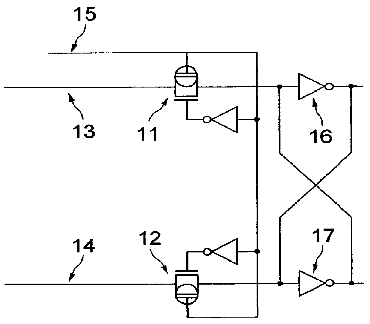
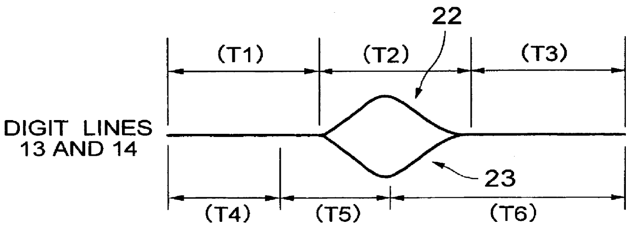
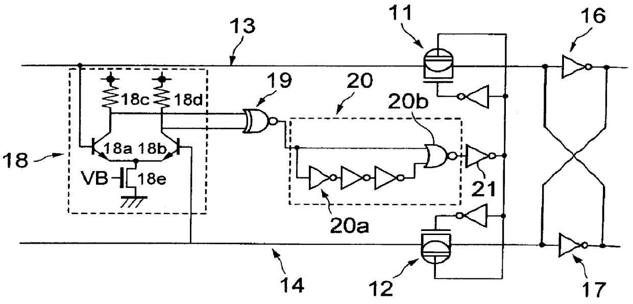
Referring to FIG. 4, a data latch circuit according to an embodiment of the present invention includes a differential amplifier 18 for detecting a potential difference between a pair of digit lines 13 and 14 which transmit a pair of complementary signals, an exclusive-NOR (Ex-NOR) gate 19 for converting the output of the differential amplifiers 18 into a digital signal, a latch timing signal generator 20 for generating a latch timing signal based on the output of Ex-NOR gate 19, inverters 21 for transmitting the output of the latch timing signal generator 20 after inversion thereof, a pair of transfer gate transistors 11 and 12 for responding to outputs from the inverters 21 to transfer the data appearing on the digit lines 13 and 14, and a flipflop section including a pair of inve...


PUM


Abstract

A data latch circuit includes a differential amplifier for detecting a potential difference between a pair of signal transmission lines for transmitting a pair of complementary signals, a latch timing signal generator for generating a latch timing signal based on the detection by the differential amplifier, and a latch section for responding to the latch timing signal to latch the complementary signals transferred thereto. A reliable and high-speed signal transmission can be achieved even in a semiconductor device having a large chip size.

Description

(a) Field of the InventionThe present invention relates to a data latch circuit and, more particularly, to a data latch circuit capable of accurately latching a data signal transferred in a semiconductor device.(b) Description of the Related ArtWith the improvement for finer patterns and high integration in semiconductor device as well as the improvement for a larger capacity therein, some of semiconductor products will have a larger chip area. In order for implementing a larger chip area along with a higher operational-speed in a semiconductor device, improvement for the signal transmission function is especially required for the semiconductor elements without generating an error signal between any locations in the larger chip area of the semiconductor device.In a semiconductor memory device, for example, a latch circuit is generally used therein as a functional element for effecting accurate take-in or latch of data. The latch circuit is provided in the semiconductor memory device...

Claims


Application Information

Patent Timeline
IPC IPC(8): H03K3/00H03K3/037G11C11/409G11C11/417G11C16/06
CPCH03K3/0375G11C7/00
Inventor HIROTA, TAKUYA
Owner RENESAS ELECTRONICS CORP
Why Eureka
Try Eureka