
Debugging system

a technology of debugging system and system, applied in the field of debugging system, can solve the problems of increasing the difficulty of debugging, affecting the quality of debugging,

Inactive Publication Date: 2000-11-07
NEC CORP
View PDF12 Cites 60 Cited by
  • Summary
  • Abstract
  • Description
  • Claims
  • Application Information

AI Technical Summary

Problems solved by technology

Recently, the system tends to become very large and complicated.
This renders software and hardware into very large sizes and makes debugging difficult more and more.
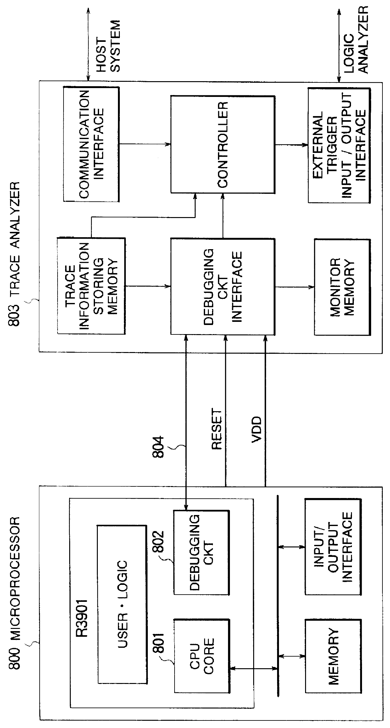
As a result, it becomes difficult to observe behavior executed in connection with an instruction, by the use of an external terminal of the LSI chip.
Under the circumstances, this structure make it difficult to analyze behavior of the timer, the serial interface, and the like from an external device and also makes it very difficult to execute debugging operation concerned with these elements.
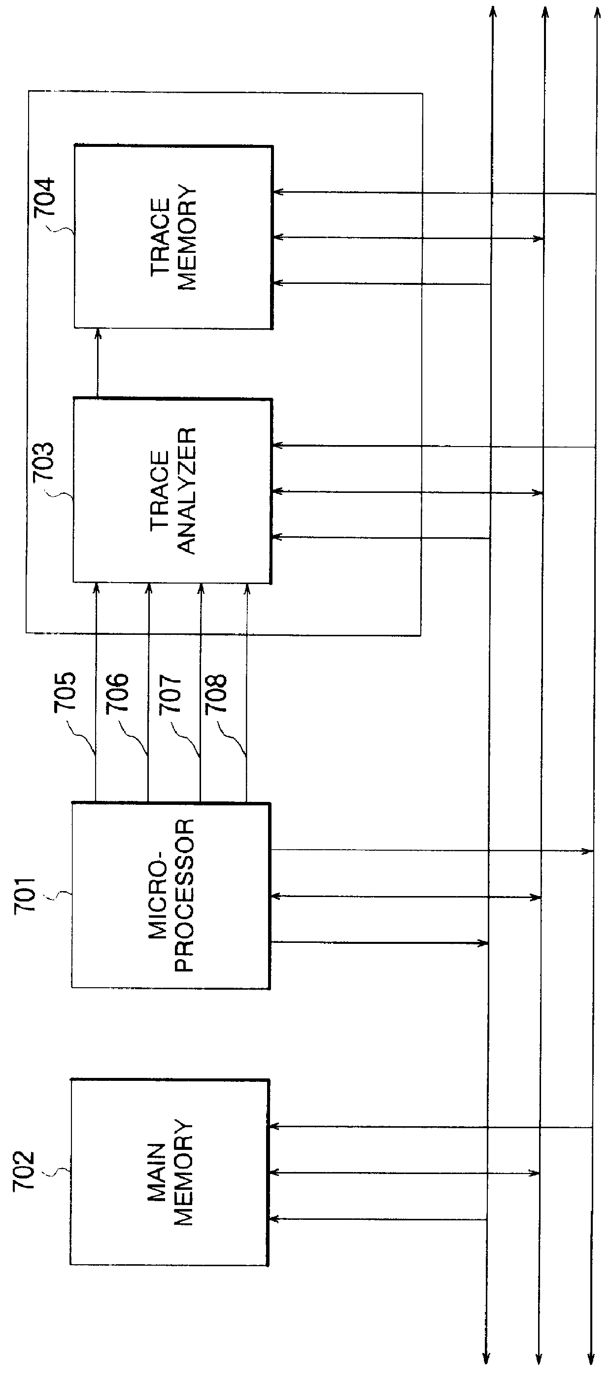
However, when the cache memory is kept in an active state, contents followed by execution of an instruction cannot be monitored by the trace analyzer 703.
Meanwhile, in a branch operation where an address is dynamically determined, estimation of the operation is not feasible only by these terminals.
However, the stoppage of the operation makes it actually impossible to observe an actual system in real time.
However, it is difficult to find out a cause of a malfunction only by the flow of the instructions, although the flow of the instructions give a clue for grasping the behavior of the system.

Method used


Image

  • Debugging system
  • Debugging system
  • Debugging system

Examples


first embodiment

FIG. 5 is a view schematically showing a debugging system according to the present invention;

FIG. 6 is a view schematically showing a probe unit shown by FIG. 5;

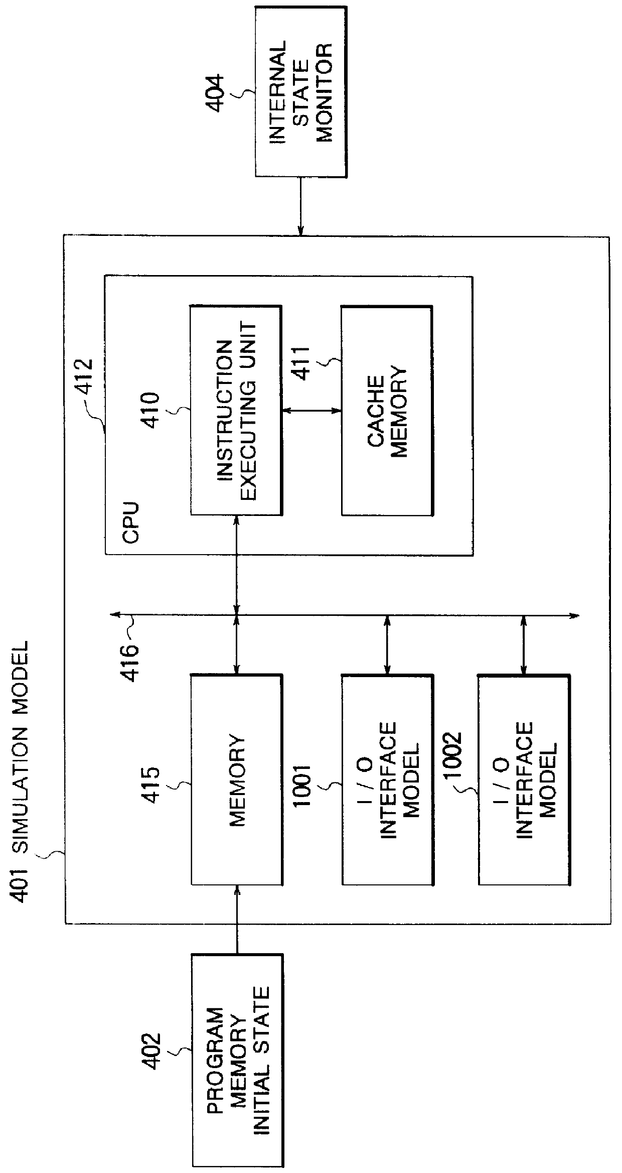
FIG. 7 is a view schematically showing a software simulation model shown by FIG. 5;

FIG. 8 is a view schematically showing another example of a probe unit according to the present invention;

FIG. 9 is a view schematically showing an example of a target system shown by FIG. 5;

FIG. 10 is a view showing an example of contents of a trace memory shown by FIG. 5;

second embodiment

FIG. 11 is a view schematically showing a debugging system according to the present invention;

FIG. 12 is a view schematically showing the structure of a probe unit 1102 of FIG. 11;

FIG. 13 is a view schematically showing a software simulator 1151 of FIG. 11;

FIG. 14 is a flowchart showing the operation of the software simulator 1151 of FIG. 11;

third embodiment

FIG. 15 is a view schematically showing a debugging system according to the present invention;

FIG. 16 is a view schematically showing the structure of a processor 1502 of FIG. 15; and

FIG. 17 is a flowchart showing the operation of a software simulator 1510 of FIG. 15.

Description will be made about the present invention in reference to the drawings hereinunder.

In FIG. 5, a debugging system is formed by a target system 1, a probe unit 2, and a software simulator model 3. Herein, the target system 1 shows an object to be debugged by the software simulator model 3 while the software simulator model 3 carries out simulation on the basis of data signals sent from the probe unit 2. In this connection, the probe unit 2 is connected to both the target system 1 and the software simulator model 3.

In the illustrated example, the target system 1 is constituted by a processor, a socket 11 of the processor, an asynchronous I / O interface 12, a main memory 13 and the like. The I / O interface 12 and t...


PUM


Abstract

In a debugging system for use in realizing simultaneously complete observation of internal operation and reproduction of malfunction actually caused in a target system which includes an integrated circuit, such as a microprocessor, contents of a memory and an internal initial state of the target system are snooped and stored in a snoop unit and a trace memory, respectively, both of which are included in a probe unit attached to the target system. The internal operation and the reproduction are simulated by a software simulator model by the use of the contents and the internal initial state which are stored in the trace memory and which are sent from the probe unit.

Description

1. Field of the InventionThe present invention relates to a debugging system for use in analyzing operation in various kinds of systems, such as an LSI system which include a microprocessor and, in particular, to a software simulator. Such systems may be, for example, a system which uses a digital synchronizing circuit wherein internal operation can not be directly monitored, a system including an interface which is located between synchronizing circuits and wherein direct monitoring of operation is difficult, or a system using an asynchronous interface such as a serial interface, a high speed bus interface or the like between synchronizing circuits.2. Description of Related ArtIn general, it is a recent trend that not only a single function but also a plurality of functions are incorporated in one chip in a functional LSI represented by a microprocessor with development of the micro fabrication technology. This enables a high speed operation of the system, a multifunction of the sy...

Claims


Application Information

Patent Timeline
IPC IPC(8): G06F11/36G06F11/34G06F11/28G06F11/22G06F11/26
CPCG06F11/3636G06F11/3632G06F11/349
Inventor SHINDOU, KEISUKE
Owner NEC CORP
Learn More