FPGA with a plurality of input reference voltage levels grouped into sets

a technology of input reference voltage and set voltage, which is applied in the field of field programmable gate arrays (fpgas), can solve the problems of inability to configure drive strength, receiver type, output driver type, and drive strength of fpgas and other ics, and achieve the effect of not allowing a user to supply an input reference voltage in the fpga

Inactive Publication Date: 2001-03-20
XILINX INC
View PDF21 Cites 2 Cited by
  • Summary
  • Abstract
  • Description
  • Claims
  • Application Information

AI Technical Summary

Benefits of technology

A configurable input / output buffer according to a first aspect of the present invention offers the advantages of compatibility with two or more different I / O standards. In one embodiment, each I / O can be separately configured. In another embodiment, several I / O are configured as a group. Therefore, a single FPGA can interface with two or more different ICs at the same time that follow two or more different I / O standards. Since the I / O standard followed by each input / output buffer can be changed by simply reconfiguring the FPGA, the resulting FPGA has a flexible input / output interface that can also adapt with the semiconductor industry to changes in I / O standards and operating voltage levels.A configurable connection of an I / O pad to one or more input reference lines allows the I / O pad to supply the input reference voltage, in accordance with a second aspect of the present invention. This aspect of the invention offers the advantages of a flexible pinout assignment in an FPGA. According to this aspect of the invention, the input reference voltage can be applied at any configurable I / O pad.A reference input that is configurably connected to any of two or more input reference voltage lines in accordance with a third aspect of the invention makes it possible to supply each of several input reference voltages to every input / output buffer in the FPGA.The separation of input reference voltages and / or output voltage supplies in accordance with fourth and fifth aspects of the invention allows an FPGA to interface relatively easily with a plurality of ICs that operate at different voltage levels.Thus it will be understood that the present invention provides an input / output interface with many novel aspects in an FPGA or a portion thereof.Those having skill in the relevant arts of the invention will now perceive various modifications and additions which may be made as a result of the disclosure herein of preferred embodiments. Accordingly, all such modifications and additions are deemed to be within the scope of the invention, which is to be limited only by the appended claims and their equivalents.

Problems solved by technology

However, as the typical gate length decreases throughout the IC industry, the typical supply voltage used in FPGAs and other ICs is decreasing.
However, in such FPGAs, factors such as output drive strength, receiver type, and output driver type are not known to be configurable to meet a particular I / O standard.
As far as is known, no FPGA allows a user to supply an input reference voltage.

Method used


Image

  • FPGA with a plurality of input reference voltage levels grouped into sets
  • FPGA with a plurality of input reference voltage levels grouped into sets
  • FPGA with a plurality of input reference voltage levels grouped into sets

Examples


Embodiment Construction

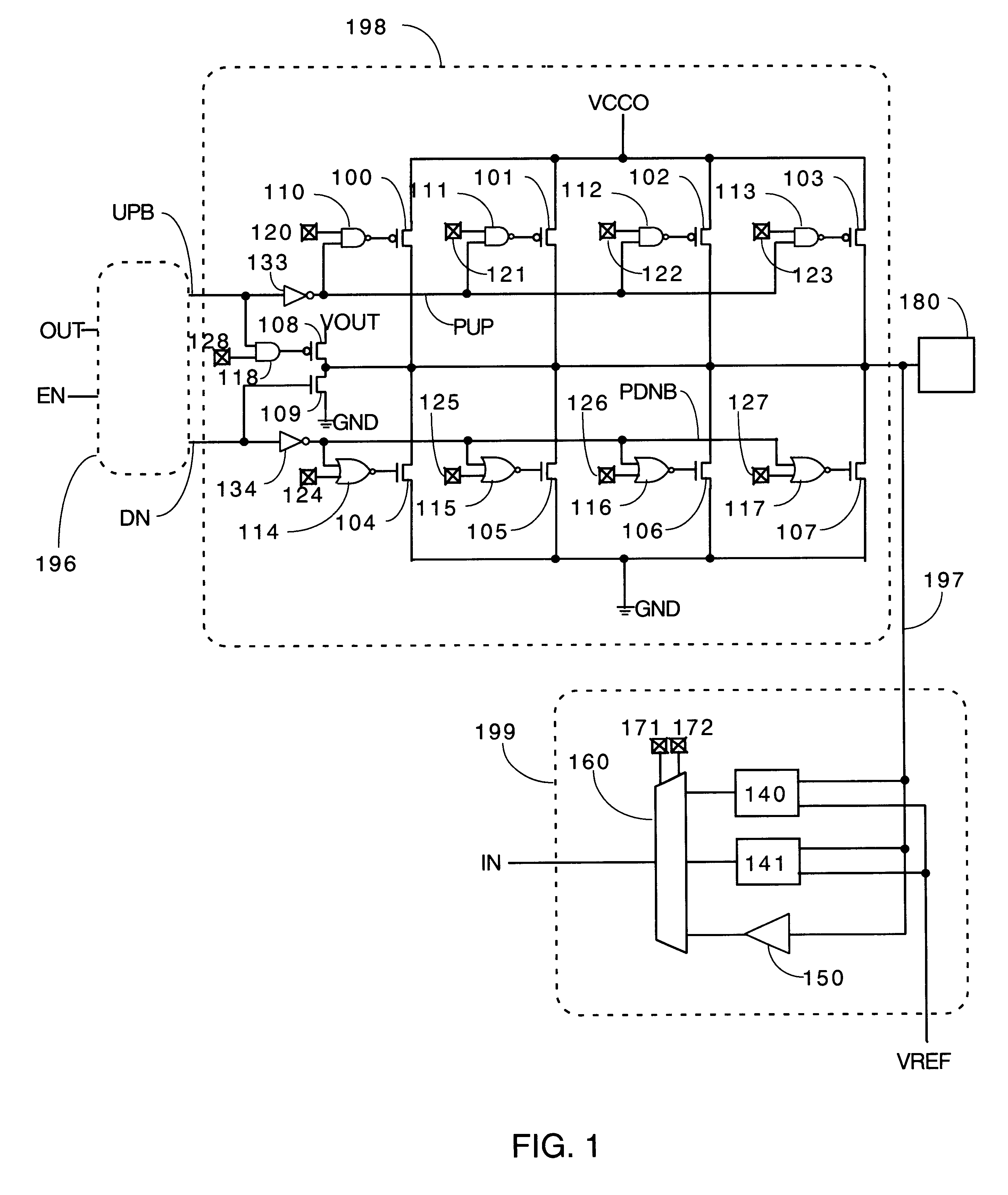
FIG. 7 shows a configurable input buffer according to a second embodiment of the invention. The input buffer of FIG. 7 resembles the input buffer of FIG. 3, except that two separate input reference voltages are supplied on input reference voltage lines VREF1 and VREF2. NMOS differential amplifier 340 compares the voltage level on pad line 197 to the input reference voltage on input reference line VREF1. PMOS differential amplifier 341 compares the voltage level on pad line 197 to the input reference voltage on input reference line VREF2.

SECOND ASPECT OF THE INVENTION

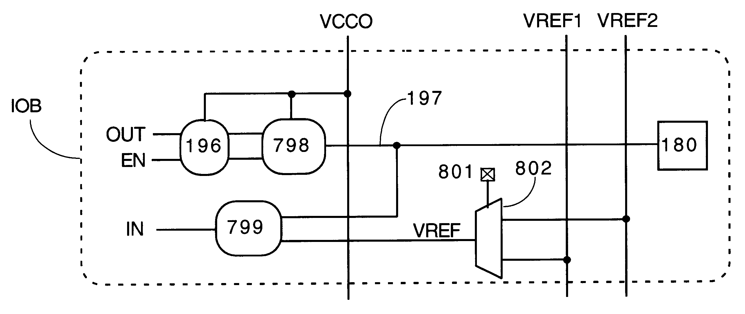
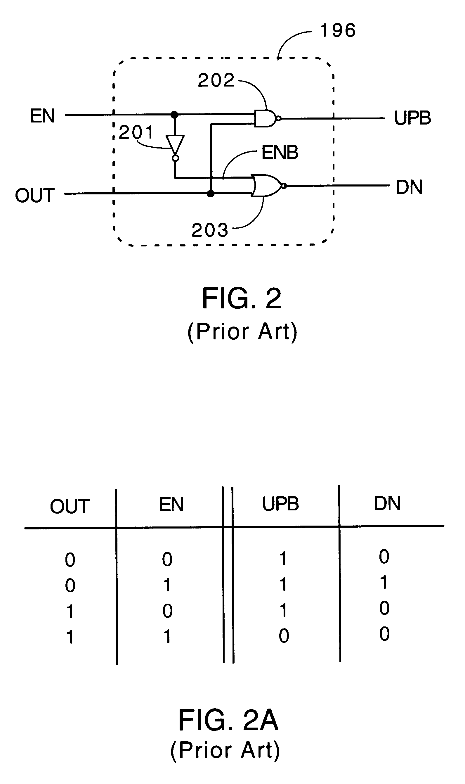
FIG. 8 shows an IOB according to a second aspect of the invention. The IOB of FIG. 8 comprises pre-driver 196, output buffer 798, pad 180 and input buffer 799. In this embodiment, I / O pad 180 can either be used to supply input reference voltage VREF, or as a signal pad. Pad line 197, which is connected to pad 180, is configurably connected to an input reference voltage line (which in this embodiment is the same as refere...


PUM


Abstract

The invention comprises an FPGA having a plurality of input reference voltages and / or output voltage supplies. In one embodiment, two or more differential amplifiers in the same configurable input buffer use different input reference voltages. According to a second aspect of the invention, the I / O pad line is configurably connected to the input reference voltage line, so that any configurable Input / Output Block (IOB) can be used to supply the input reference voltage. According to a third aspect of the invention, the reference input of an I / O is configurably connected to any of two or more input reference voltage lines. According to another aspect of the invention, a single input reference voltage and / or a single output voltage supply is applied to each IOB, with the IOBs grouped into sets. Each set of IOBs has a separate input reference voltage and / or a separate output voltage supply.

Description

1. Field of the InventionThe invention relates to Field Programmable Gate Arrays (FPGAs). More particularly, the invention relates to input / output (I / O) voltage levels in an FPGA.2. Description of the Background ArtExisting I / O structures for integrated circuits (ICs) are typically designed to function according to a specific I / O standard. There are several different I / O standards in use, and new standards are often introduced. These I / O standards typically include such factors as output drive strength, receiver type, output driver type, and output signal slew rate. One such I / O standard is the GTL+ standard, described in pages 46 through 50 of the Pentium Pro Processor data sheet entitled "PENTIUM PRO PROCESSOR AT 150 MHz, 166 MHz, 180 MHz and 200 Mhz", published Nov. 1995 and available from Intel Corporation, 2200 Mission College Blvd., Santa Clara, Calif. 95052-8119, which are incorporated herein by reference. ("Pentium" is a registered trademark owned by Intel Corporation.)A typ...

Claims


Application Information

Patent Timeline
Patent Type & Authority Patents(United States)
IPC IPC(8): G06F7/38H03K19/177H03K19/094H03K19/003
CPCH03K19/00361H03K19/17744H03K19/1778H03K19/17788
Inventor GOETTING, F. ERICHFRAKE, SCOTT O.KONDAPALLI, VENU M.YOUNG, STEVEN P.
Owner XILINX INC
Why Eureka
Try Eureka