Method of driving electron-emitting device, method of driving electron source using the electron-emitting device, and method of driving image forming apparatus using the electron source

a technology of electron emission device and electron source, which is applied in the field of flat panel display, can solve the problems of increasing the severity of the phenomenon, the inability to maintain the atmosphere formed in the stabilization step, and the current of the device if and the emission current become unstabl

Inactive Publication Date: 2001-05-01
CANON KK
View PDF22 Cites 60 Cited by
  • Summary
  • Abstract
  • Description
  • Claims
  • Application Information

AI Technical Summary

Problems solved by technology

However, LCD is not of a emissive type, and must be equipped with a backlight.
However, it is difficult to maintain the atmosphere formed in the stabilization step and to form an atmosphere desired in the stabilization step.
In addition, the device current If and emission current Ie become unstable.
This phenomenon becomes more serious in an electron source in which a plurality of devices are connected to a common wiring.
In this case, however, the maximum voltage value (Vmax) maybe unnecessarily applied.
When the maximum voltage value (Vmax) is periodically applied to all the devices at a predetermined interval, it is undesirably applied to a device which does not vary in characteristic or exhibits only a small degree of variation.
However, the device characteristic may greatly deteriorate due to an unnecessarily long application time of the maximum voltage value (Vmax) in a device which does not vary in characteristic or exhibits only a small degree of variation.
However, this classification is not strict and changes depending on a target property.
However, the device characteristic to which the driving method of the embodiment can be adopted is the MI characteristic of monotonically increasing the device current If with respect to the device voltage Vf.
Further, the device current If and emission current Ie with respect to a predetermined device voltage Vf become unstable.

Method used


Image

  • Method of driving electron-emitting device, method of driving electron source using the electron-emitting device, and method of driving image forming apparatus using the electron source
  • Method of driving electron-emitting device, method of driving electron source using the electron-emitting device, and method of driving image forming apparatus using the electron source
  • Method of driving electron-emitting device, method of driving electron source using the electron-emitting device, and method of driving image forming apparatus using the electron source

Examples


example 2

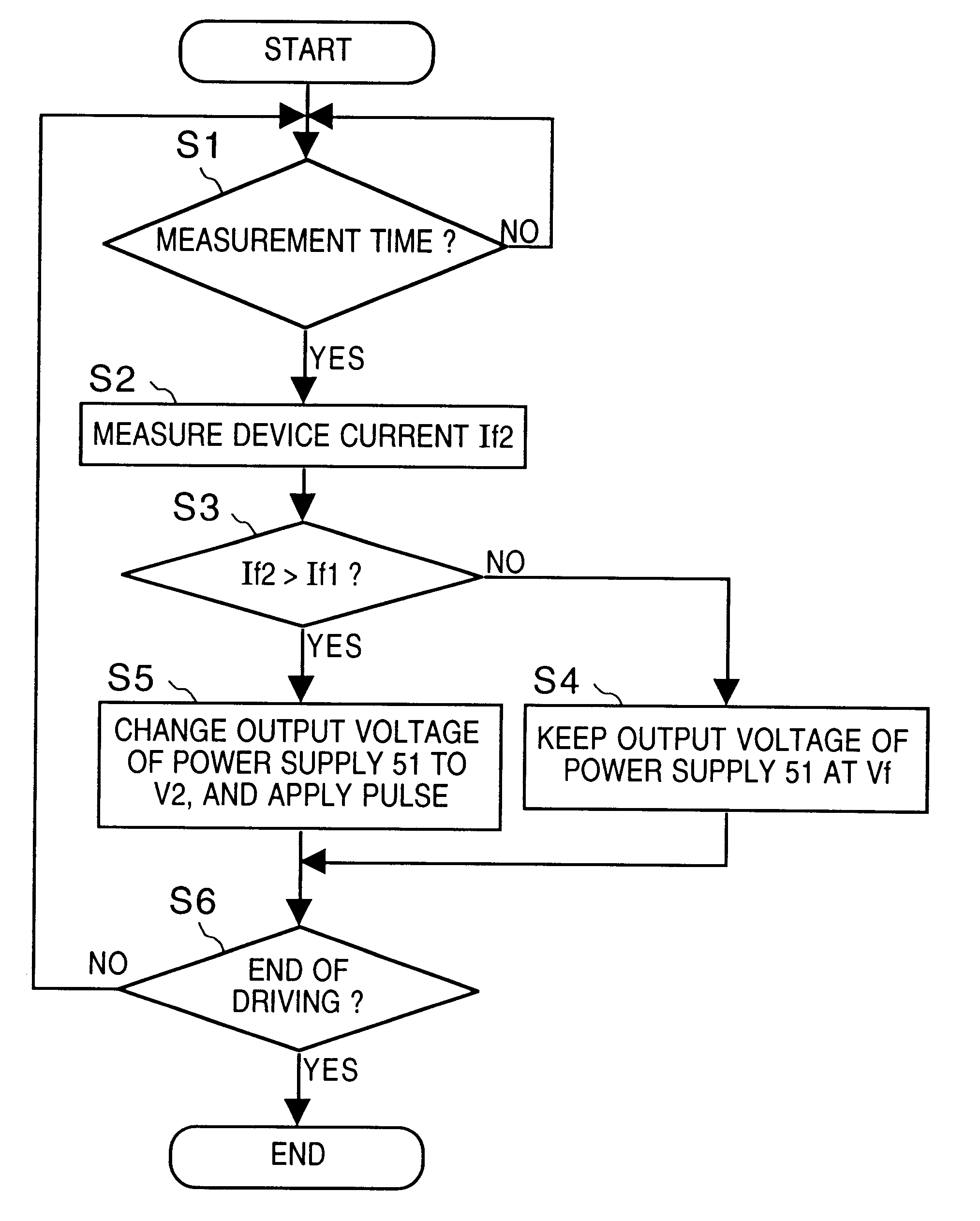
A device C was formed by the same process as in Example 1 up to the stabilization step.

Even after the stabilization step, while the vacuum degree was maintained, the device C was applied a voltage to measure the device current If and emission current Ie.

The waveform shown in FIG. 4A was used for the device C. The pulse width T1 and pulse interval T2 were respectively set to 0.2 msec and 10 msec, and three pulses having a peak value of 15 V were applied to measure the emission current Ie. The pulse width T1 and pulse interval T2 were respectively set to 0.2 msec and 10 msec, and three pulses having a peak value of 14 V were applied to measure the emission current Ie (first measurement step). As a result, the emission current Ie was about 40% the emission current obtained by applying the pulse having a peak value of 15 V. Therefore, when a pulse having a peak value of 15 V was applied, the pulse width was set about 40% that for a peak value of 14 V. With this setting, charges captured...

example 3

In Example 3, an image forming apparatus like the one shown in FIG. 9 was fabricated using an electron source (FIG. 8) obtained by arranging a plurality of electron-emitting devices shown in FIGS. 20A and 20B. An application of the driving method of Example 3 will be described.

FIG. 16 is a plan view showing part of a substrate 71 on which a plurality of electron-emitting devices 74 are laid out in a matrix. Th electron source of the image forming apparatus in Example 3 is constituted by laying out a plurality of electron-emitting devices shown in FIGS. 20A and 20B in a matrix.

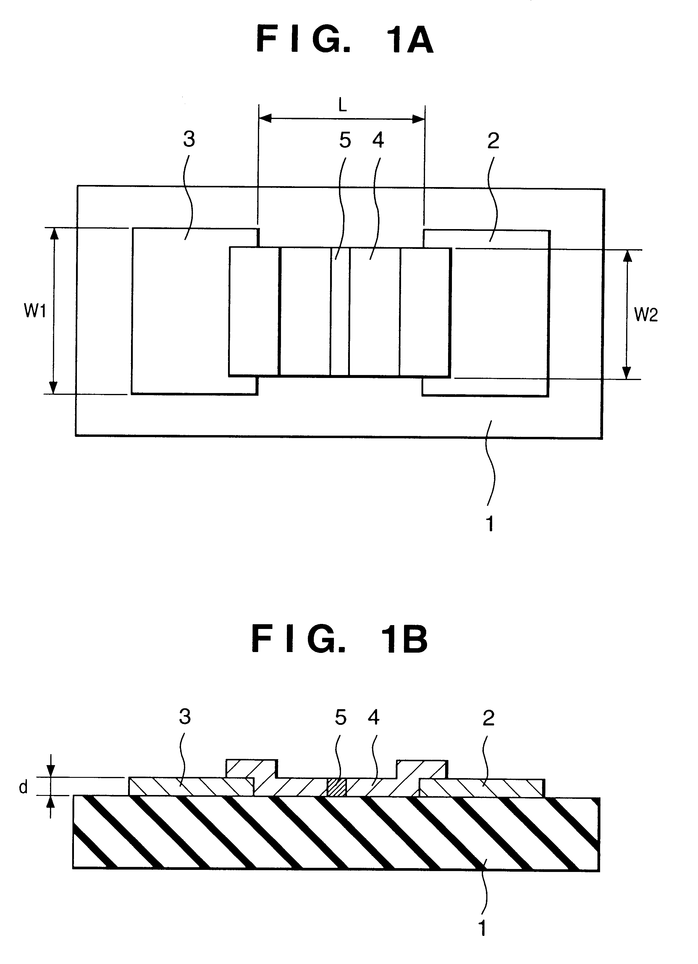
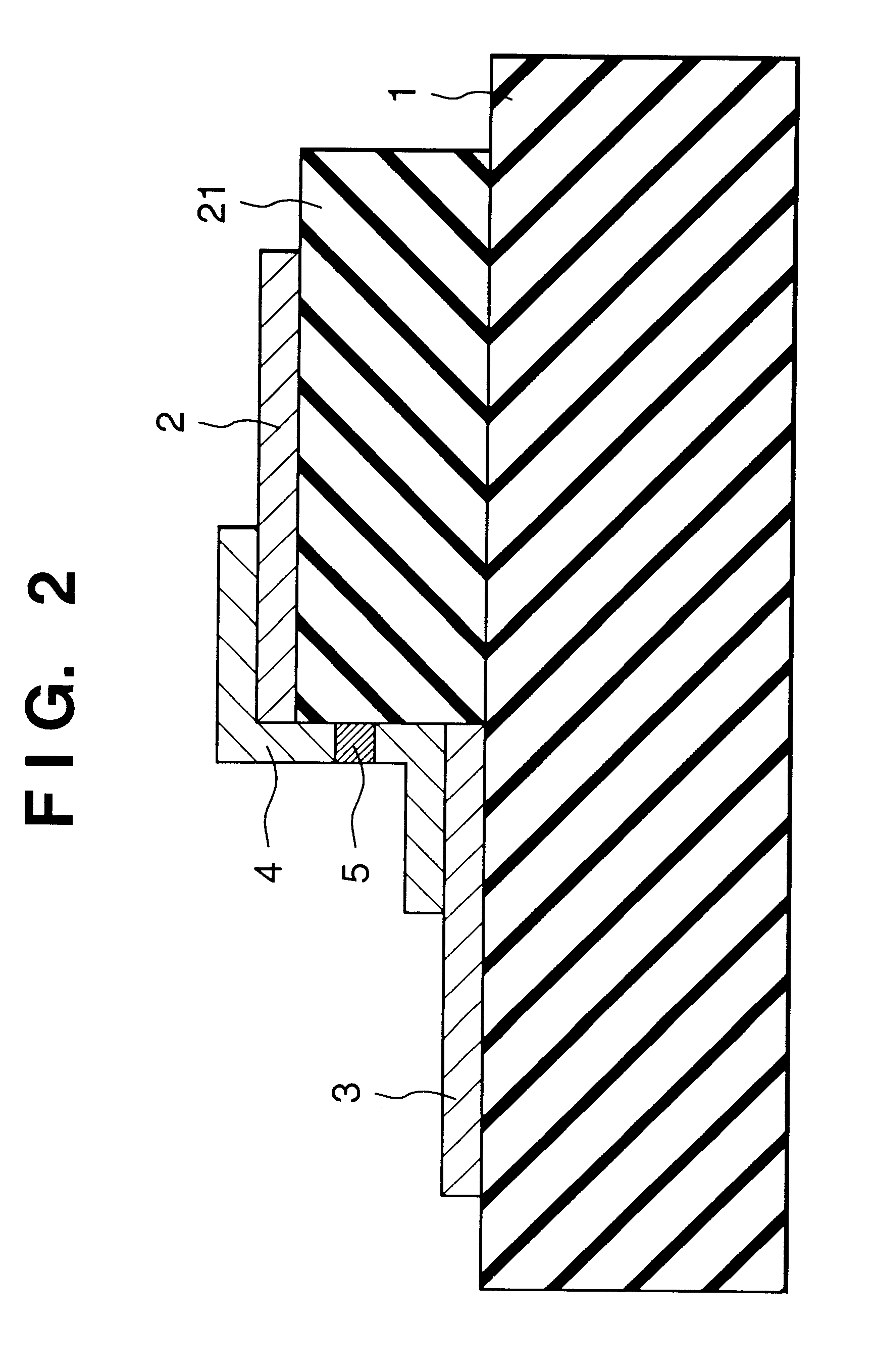
FIG. 17 is a sectional view taken along the line A-A' in FIG. 16. In FIGS. 16 and 17, the same reference numerals denote the same parts. In FIGS. 16 and 17, reference numeral 1 denotes a substrate; 72, x-direction wirings (lower wirings) corresponding to Doxm in FIG. 9; 73, y-direction wirings (upper wirings) corresponding to Doyn in FIG. 9; 4, a conductive film; 2 and 3, electrodes; 131, an interlevel insulati...

example 4

In Example 4, a flat panel display was manufactured. A display panel 101 constituting the flat panel display of Example 4 was prepared similarly to Example 3 (step-a to step-n) (FIG. 9).

The driving method of Example 4 will be described. FIG. 23 shows a driving circuit in Example 4. In FIG. 23, the same reference numerals denote the same parts of the basic driving circuit shown in FIG. 13.

In FIG. 23, the display panel 101 is connected to an external electric circuit via terminals Dox1 to Doxm and Doy1 to Doyn. A high-voltage terminal Hv on a face plate is connected to an external high-voltage power supply Va. The terminals Dox1 to Doxm receive scan signals for sequentially driving a multi electron source incorporated in the panel, i.e., electron-emitting devices laid out in a m.times.n matrix in units of lines. The terminals Dy1 to Dyn receive modulation signals for controlling electron beams output from the electron-emitting devices on one line selected by the scan signals.

The scan ...


PUM


Abstract

An emission current (Ie1) emitted by the electron-emitting device and/or a device current (If1) flowing through the electron-emitting device are measured when a voltage (V1) is applied to the electron-emitting device and an emission current (Ie2) emitted by the electron-emitting device and/or a device current (If2) flowing through the electron-emitting device are measured when the voltage (V1) is applied to the electron-emitting device after the measurement step. A voltage (V2) higher than the voltage (V1) is applied to the electron-emitting device when the emission current (Ie2) is larger than the emission current (Ie1) and/or the device current (If2) is larger than the device current (If1).

Description

1. Field of the InventionThe present invention relates to a flat panel display and, more particularly, to a method of driving an electron-emitting device, a method of driving an electron source formed by arranging a plurality of electron-emitting devices, and a method of driving an image forming apparatus using the electron source.2. Description of the Related ArtConventionally, two types of devices, namely thermionic cathode and cold cathode, are known as electron-emitting devices. Known examples of the cold cathodes are surface-conduction emission type electron-emitting devices, field emission type electron-emitting devices (to be referred to as FE type electron-emitting devices hereinafter), and metal / insulator / metal type electron-emitting devices (to be referred to as MIM type electron-emitting devices hereinafter).A known example of the surface-conduction emission type electron-emitting devices is described in, e.g., M. I. Elinson, "Radio Eng. Electron Phys., 10, 1290 (1965).Th...

Claims


Application Information

Patent Timeline
Patent Type & Authority Patents(United States)
IPC IPC(8): G09G3/22H01J31/12G09G3/20H01J1/316
CPCG09G3/22H01J31/127G09G3/2014G09G2310/0275G09G2320/04G09G2320/043H01J2201/3165
Inventor KOBAYASHI, TAMAKISUZUKI, NORITAKE
Owner CANON KK
Why Eureka
Try Eureka