Wafer edge deposition elimination

a wafer edge and deposition technology, applied in the direction of electrolysis components, vacuum evaporation coatings, coatings, etc., can solve the problems of incomplete shadowing of the wafer edge, failure of purge gas ring, failure of shadow ring,

Inactive Publication Date: 2001-05-15
APPLIED MATERIALS INC
View PDF15 Cites 58 Cited by
  • Summary
  • Abstract
  • Description
  • Claims
  • Application Information

AI Technical Summary

Benefits of technology

Thus, the shadow ring inhibits deposition of process gases on the wafer in two distinct ways. First, the shadow ring physically obstructs process gas, flowing down from above the wafer, from depositing on the masked portion of the wafer. Second, the shadow ring is used to direct purge gas flow to inhibit process gas from seeping under the shadow ring and depositing near the wafer edge.
Six alignment pins are pressed into and protrude from the wafer supporting surface of the heater pedestal. These pins have sloping surfaces and are arranged so that they guide the wafer to a centered position on the heater pedestal when the wafer is placed on the pedestal. These pins are preferably made from a material which minimizes friction between the pins and the wafer, so that the wafer slides easily into position.
The shadow ring typically also has lower thermal conductivity than the heater pedestal, which reduces heat transfer from the heater pedestal to the shadow ring. As the rate of deposition is temperature-dependent, reducing the temperature of the shadow ring reduces deposition thereon. In a preferred embodiment, the heater pedestal is made of aluminum, the support ring is made of 6061-T6 aluminum alloy, and the shadow ring is made of 314 stainless steel or a ceramic.
The heat transfer is further inhibited by minimizing the contact area between the support ring and the shadow ring, which may be accomplished by designing the two rings to have minimal overlap.
One advantage of this invention is that it substantially eliminates the occurrence of deposition near the edge of the wafer. This in turn eliminates particle contaminants originating from unwanted near-edge deposition that inadequately adheres to the surface.
Another advantage of this invention is that the aligning pins serve to align the wafer with the pedestal, the shadow ring with the pedestal, and thus, the shadow ring with the wafer. This prevents "off centered" shadowing of the edge portion of the wafer, as well as incomplete shadowing of a non-circular wafer by a non-circular shadow ring that is rotationally misaligned with respect to the wafer.

Problems solved by technology

In practice, however, the purge gas ring is not as successful as might be desired.
However, the shadow ring is also not as successful as might be desired because of wafer warpage and the fact that the volatile deposition gas still tends to migrate under the lip of the shadow ring and deposit unwanted material on the wafer edge and backside.
Furthermore, any misalignment of the shadow ring with respect to the wafer may result in incomplete shadowing of the wafer edge.
First, the shadow ring physically obstructs process gas, flowing down from above the wafer, from depositing on the masked portion of the wafer.

Method used


Image

  • Wafer edge deposition elimination
  • Wafer edge deposition elimination
  • Wafer edge deposition elimination

Examples


Embodiment Construction

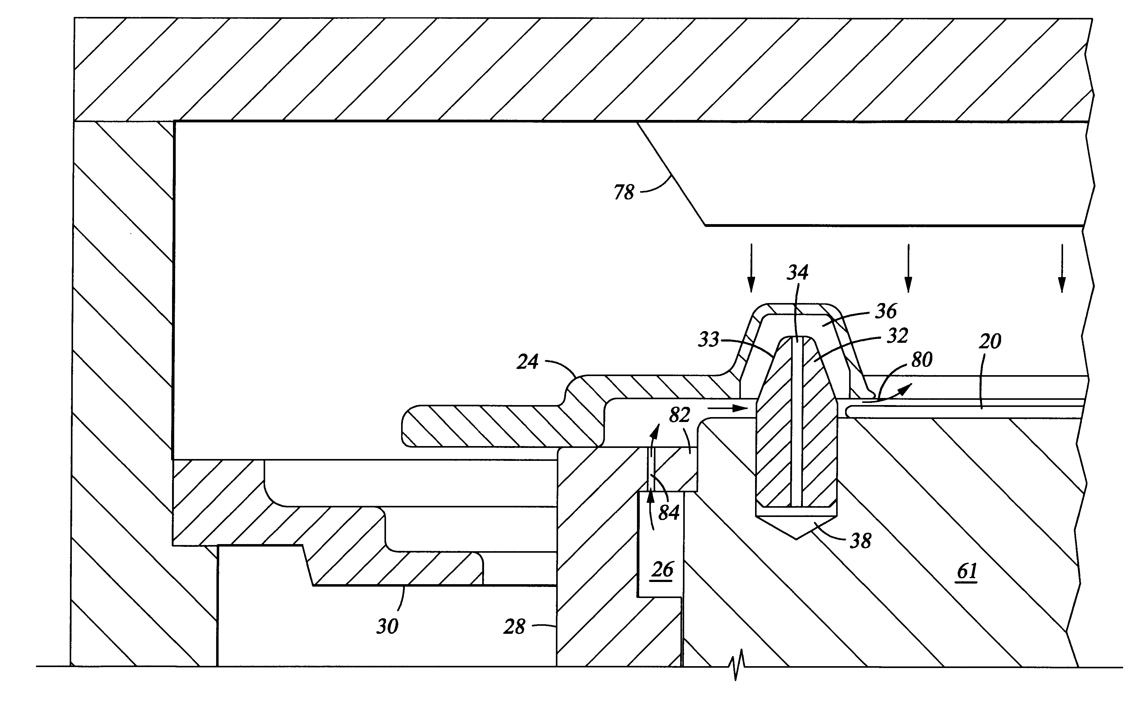
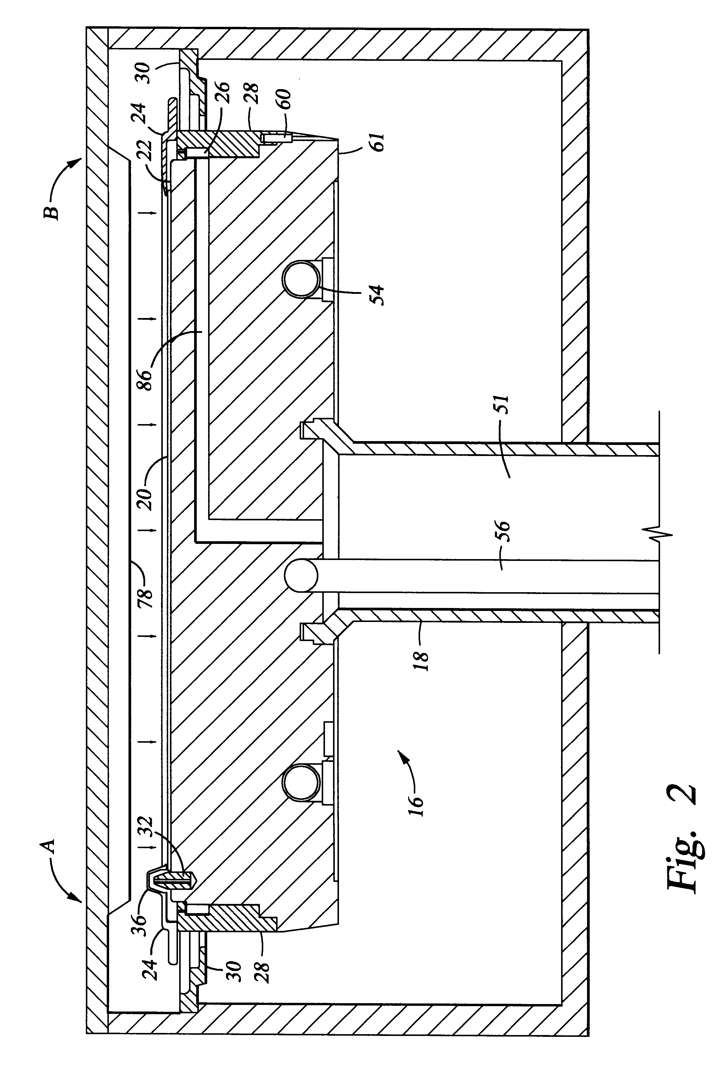
1. Pedestal and Shadow Ring Architecture

In FIG. 2, a heater pedestal 16 is shown to comprise a main body 61 supported by a vertical stalk 18. Within the stalk 18 are a purge gas conduit 51, a housing containing a thermocouple (not shown) for measuring the temperature of the pedestal, and a conduit 56 for supplying power to a heating element 54 located within the main body 61 of the pedestal 16. The main body 61, which is typically made from aluminum, has a supporting surface 22 on which a semiconductor wafer can be supported. The surface 22 of the pedestal 16 may have formed therein a plurality of concentric vacuum grooves (not shown) for applying a vacuum to draw the wafer 20 onto the supporting surface 22 for improved uniformity of heating during operation. These vacuum grooves may take the form of concentric grooves and be supplied by a vacuum conduit (not shown) as described in pending U.S. patent application Ser. No. 08 / 626,789. The surface 22 may be textured to reduce the area...


PUM

PropertyMeasurementUnit
temperatureaaaaaaaaaa
operating temperatureaaaaaaaaaa
angleaaaaaaaaaa

Abstract

This invention provides a method and apparatus for substantially eliminating deposition on the edge of a wafer supported on a pedestal in a processing chamber. Process gas flow onto the wafer surface is inhibited from reaching the wafer edge and backside, by means of a shadow ring placed over the wafer without touching it. Deposition on the edge and backside of the wafer are therefore substantially eliminated. The shadow ring defines a cavity which circumscribes the wafer edge, into which purge gas is flowed. This purge gas flows out from the cavity through the gap between the shadow ring and the upper surface of the wafer. Alignment pins are placed on the wafer supporting surface of the pedestal. These pins have sloping surfaces and are arranged to guide the wafer to a centered position on the pedestal when the wafer is placed on the pedestal. These pins also serve to align the shadow ring to the pedestal and thence to the wafer. The shadow ring has a plurality of keyed formations which mate to the pins, and as the shadow ring and pedestal are brought together, the pins serve to align the shadow ring. This precise rotational alignment and centering of the shadow ring results in substantial elimination of edge deposition. The keyed formations have elliptical cross-sections to provide for radial movement of the pins with respect to the keyed formations due to thermal expansion.

Description

1. Field of the InventionThis invention relates to a method and apparatus for depositing useful layers of materials on substrates, for example, semiconductor wafers, used in the manufacture of semiconductor dies. More particularly, this invention relates to a method and apparatus for substantially eliminating unwanted deposition on the edge of the wafer.2. BackgroundOverview of Chemical Vapor DepositionChemical vapor deposition, commonly referred to as "CVD," is one of a number of processes used to deposit thin layers of material on a semiconductor wafer, and may be based on thermal, plasma, or optically assisted decomposition, or reaction of chemicals. To process wafers in, for example, a thermal CVD process, a chamber is provided with a susceptor configured to receive a wafer. The wafer is typically placed onto and removed from the susceptor by a robot blade and supported by the susceptor during processing. In these typical systems, the susceptor and the wafer are heated to a temp...

Claims


Application Information

Patent Timeline
Patent Type & Authority Patents(United States)
IPC IPC(8): C23C16/46C23C16/458C23C16/44C23C16/455
CPCC23C16/45521C23C16/458C23C16/4583C23C16/4585C23C16/46Y10S156/916
Inventor CHEN, AIHUALITTAU, KARL A.ZHOU, DASHUN S.
Owner APPLIED MATERIALS INC
Why Eureka
Try Eureka