Method and apparatus for biasing a CMOS active pixel sensor above the nominal voltage maximums for an IC process

a cmos active pixel and ic process technology, applied in the field of cmos active pixel sensors, can solve the problems of insufficient sensing of the brightest levels in the dynamic range corresponding to the highest levels of captured photocharge, and the shrinking of process technology and the corresponding nominal operating voltage of the components in the integrated circui

Inactive Publication Date: 2001-06-12
FOVEON
View PDF57 Cites 86 Cited by
  • Summary
  • Abstract
  • Description
  • Claims
  • Application Information

AI Technical Summary

Problems solved by technology

Unfortunately, the shrinking of the process technology and the corresponding nominal operating voltages of the components in the integrated circuit are not directly scalable in some integrated circuit applications in the sense that the integrated circuit will not operate as desired for the nominal voltages that are typically indicated for the process technology by which...

Method used


Image

  • Method and apparatus for biasing a CMOS active pixel sensor above the nominal voltage maximums for an IC process
  • Method and apparatus for biasing a CMOS active pixel sensor above the nominal voltage maximums for an IC process
  • Method and apparatus for biasing a CMOS active pixel sensor above the nominal voltage maximums for an IC process

Examples


Embodiment Construction

Those of ordinary skill in the art will realize that the following description of the present invention is illustrative only and not in any way limiting. Other embodiments of the invention will readily suggest themselves to such skilled persons.

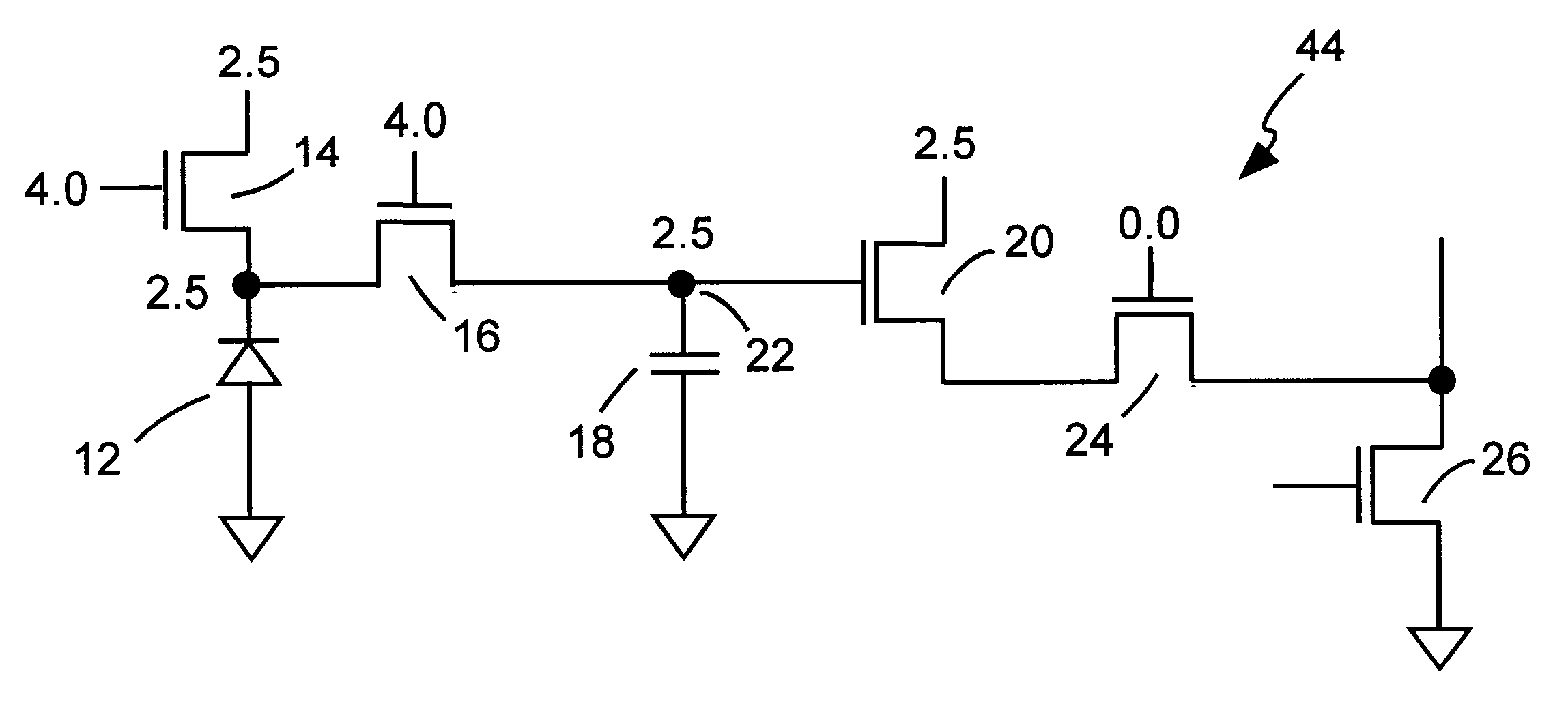
According to the present invention, an active pixel sensor that it is fabricated with, for example, a 0.25 um CMOS process is coupled to operating voltages which are above the nominal operating voltage for the process technology to provide a useful dynamic range.

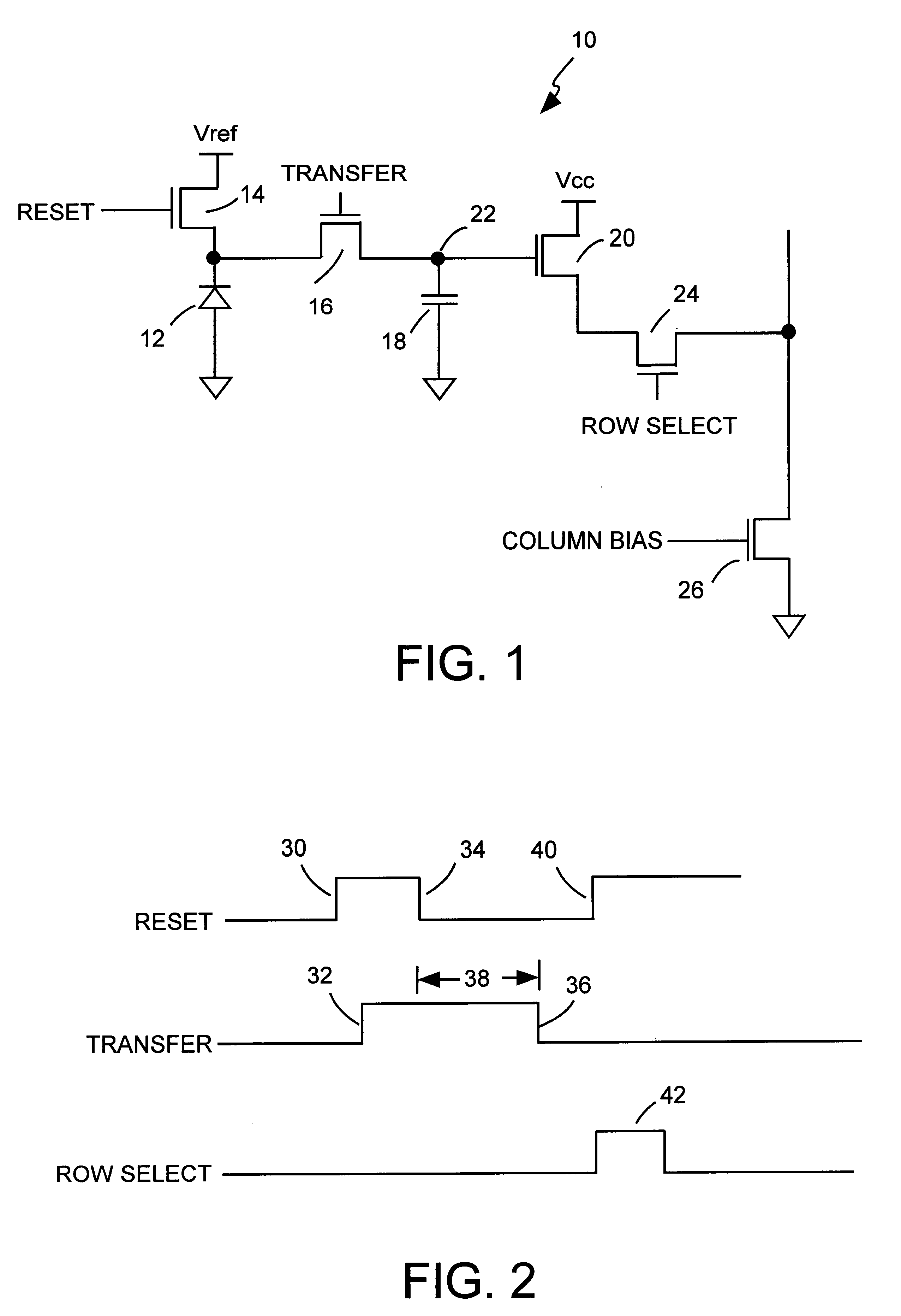
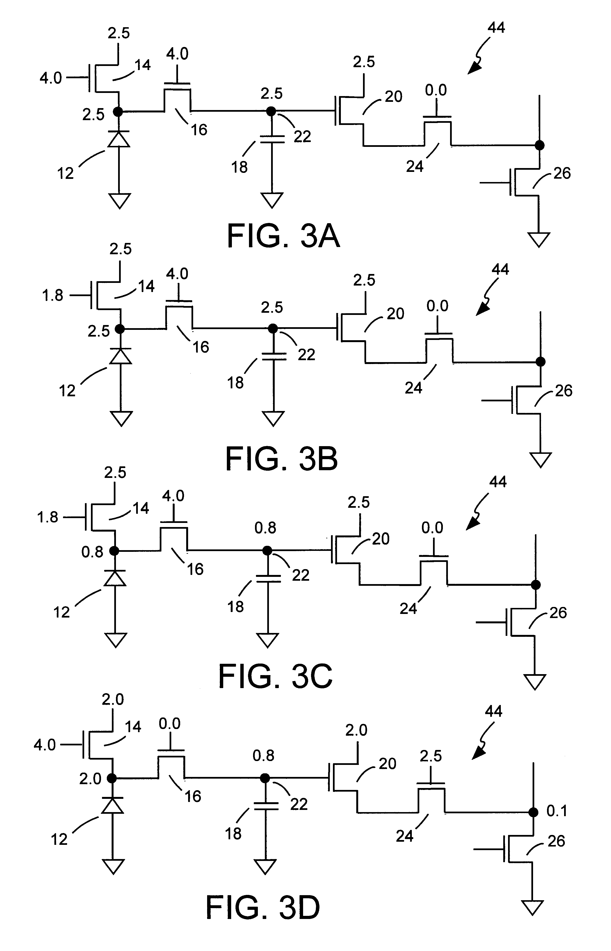
In FIGS. 3A through 3D the nominal voltages at which an active pixel sensor 44 is operated according to the present invention are illustrated. The active pixel sensor 44 is similar to the active pixel sensor 10 depicted in FIG. 1, accordingly, in each of the FIGS. 3A through 3D, the elements therein employ the reference numerals depicted in FIG. 1 for the same elements. In the operation of the active pixel sensor 44, FIG. 3A corresponds to the reset period, FIGS. 3B and 3C correspond ...


PUM


Abstract

An active pixel sensor is operated with voltages that exceed the nominal operating voltages for a particular integrated circuit process. Voltages that exceed the nominal operating voltages are employed during the reset, integration and readout periods in the operating cycle of the active pixel sensor. The lower limit of the voltage representing the capture of photocharge in the active pixel sensor is fixed by setting the voltage applied to the gate of a reset transistor in the active pixel sensor to a level during integration which prevents the voltage across the dielectric of a transfer transistor from exceeding a preselected value. Read disturb caused by impact ionization current from a readout transistor to a storage node is reduced by lowering the voltage applied to the drain of a readout transistor to reduce the Vds of the readout transistor at the start of a readout period.

Description

1. Field of the InventionThe present invention relates to CMOS active pixel sensors. More particularly, the present invention relates to biasing a CMOS active pixel sensor at voltages that exceed the nominal voltage maximums of the CMOS active pixel sensor to maximize the dynamic range in the CMOS active pixel sensor. Further, the present invention relates to biasing to reduce read disturb resulting from impact ionization current phenomenon in the CMOS active pixel sensor.2. The Related ArtIt can be readily observed by those of ordinary skill in the art that the size of the components and interconnect between components in integrated circuits have steadily decreased to permit a greater number of circuits to be formed on a single piece of silicon. As the process technologies shrink the size of the components and interconnect in an integrated circuit, a corresponding decrease in the nominal operating voltages of the components in integrated circuits have also decreased. Unfortunately,...

Claims


Application Information

Patent Timeline
IPC IPC(8): H04N5/217H04N3/15H04N5/355H04N5/363H04N5/374
CPCH04N5/363H04N5/374H04N25/65H04N25/76
Inventor MERRILL, RICHARD B.
Owner FOVEON
Why Eureka
Try Eureka