Multi-value logic device, bus system of multi-value logic devices connected with shared bus, and network system of information processors loaded with multi-value logic devices and connected with shared network

a logic device and multi-value technology, applied in the field of multi-value logic devices, can solve the problems of deterioration of reliability, cost increase, and inability to reduce the bus width

Inactive Publication Date: 2001-07-24
MITSUBISHI ELECTRIC CORP
View PDF5 Cites 25 Cited by
  • Summary
  • Abstract
  • Description
  • Claims
  • Application Information

AI Technical Summary

Problems solved by technology

Therefore, with the increase of bus width and, accordingly, with the increase of the number of pins or wiring, the enlargement of a device, a board loaded with the device and further an equipment itself loaded with the board, the deterioration of reliability due to complicated wiring, or the cost increase, has caused problems.
However, in the technique in which the transfer of binary data is a prerequisite, the bus width cannot be reduced.
In the bus system in which conventional multi-value logic devices are connected, however, since the devices use the same bus levels in the system, communication cannot be executed simultaneously with other communication to avoid mutual interference as long as the shared bus is used.
Therefore, multiplex communication by a plurality of bus masters is impossible, so that throughput cannot be enhanced.

Method used


Image

  • Multi-value logic device, bus system of multi-value logic devices connected with shared bus, and network system of information processors loaded with multi-value logic devices and connected with shared network
  • Multi-value logic device, bus system of multi-value logic devices connected with shared bus, and network system of information processors loaded with multi-value logic devices and connected with shared network
  • Multi-value logic device, bus system of multi-value logic devices connected with shared bus, and network system of information processors loaded with multi-value logic devices and connected with shared network

Examples


first embodiment

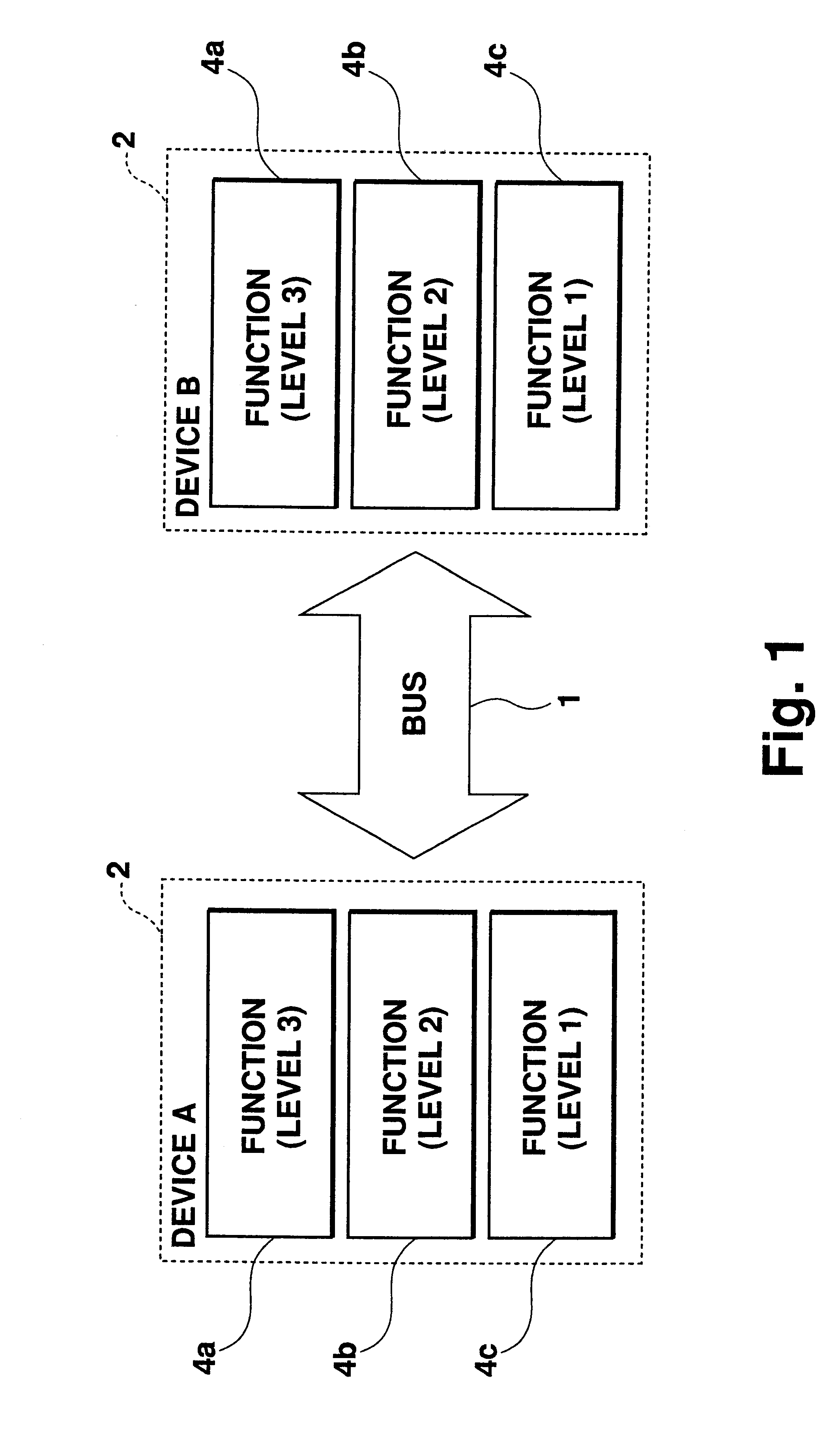
FIG. 1 is a diagram showing the overall structure of a bus system according to the present invention. The bus system is usually provided in an information processor such as a computer. FIG. 1 shows a pair of devices 2 connected via a bus 1. The device 2 is a multi-value logic device which converts binary logic signals outputted from functions 4a, 4b, 4c mounted therein to an analog multi-value logic signal to perform data transfer.

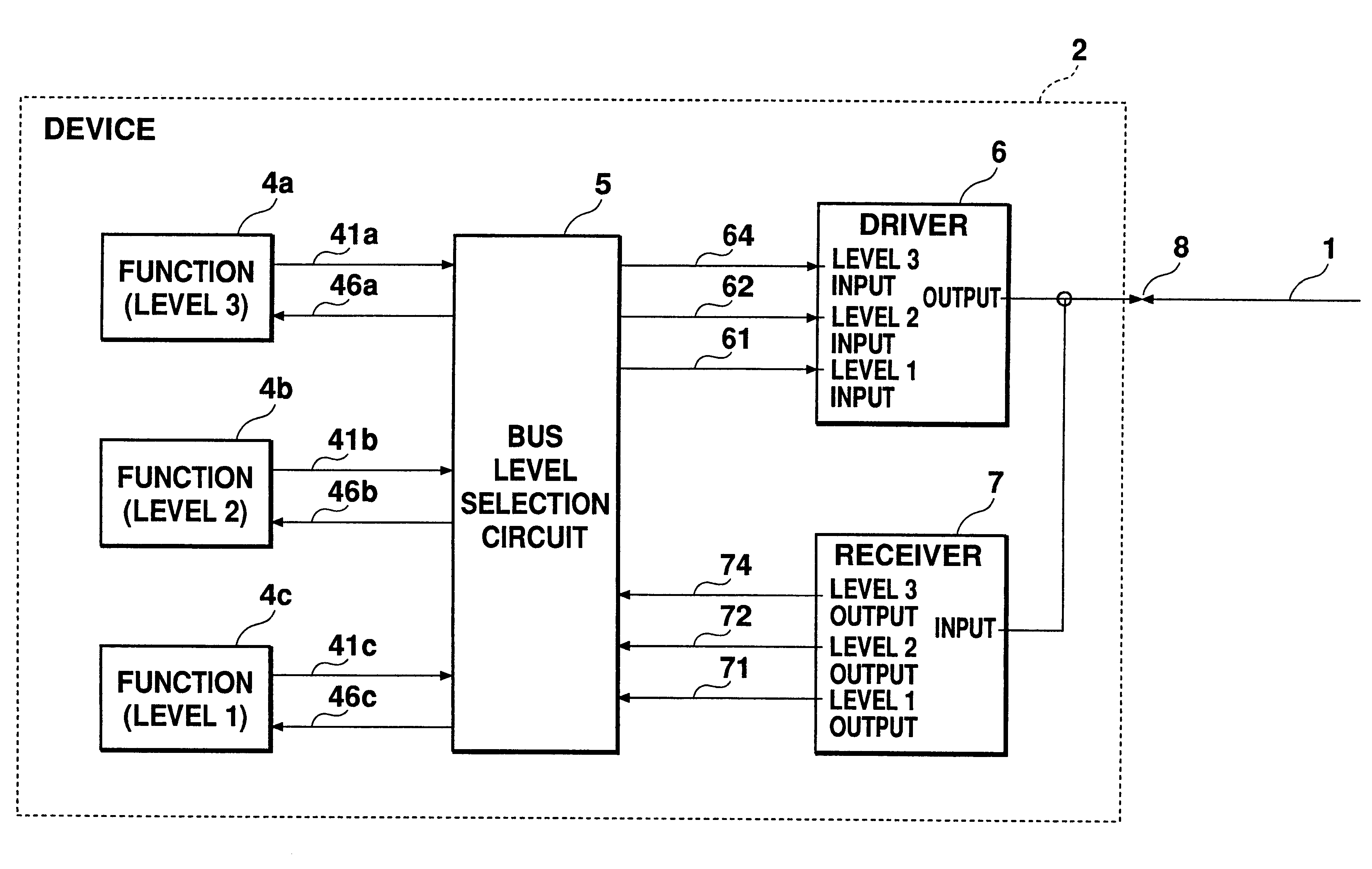
FIG. 2 is a block diagram showing the inside of the device in the first embodiment. The device 2 has the functions 4a, 4b, 4c, a bus level selection circuit 5, a driver 6 and a receiver 7. The device 2 is connected to the bus 1 shared by the devices via an input / output pin 8.

The functions 4a, 4b, 4c realize, for example, a SCSI .Th10 controller, a network controller, a cache controller and other functions of the device 2. In the embodiment, the device 2 has a plurality of functions. The functions 4a, 4b, 4c transmit signals 41a, 41b, 41c to the bus level s...

second embodiment

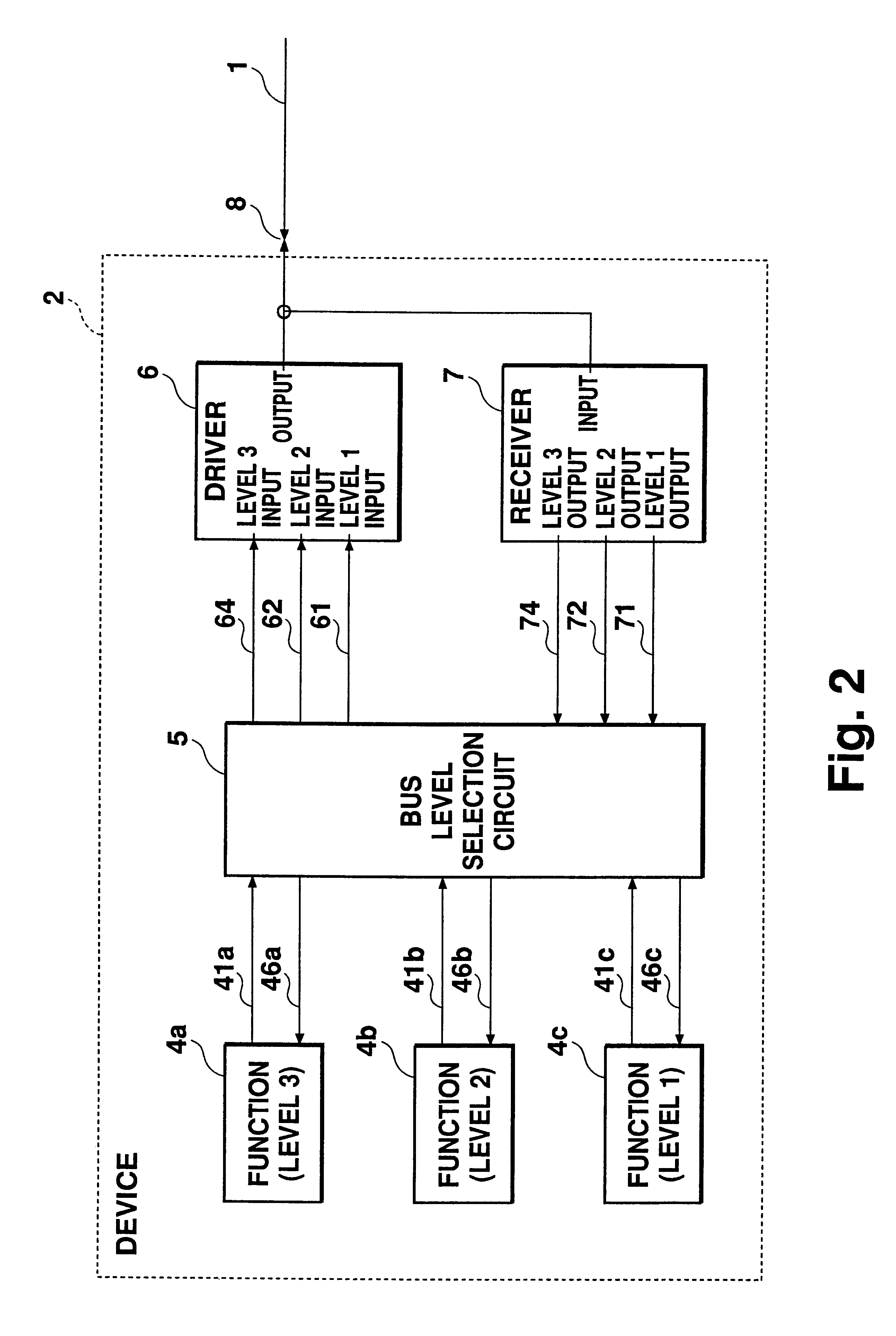
FIG. 5 is a block diagram showing the internal structure of a multi-value logic device according to the second embodiment of the present invention. Additionally, the same structure and signals as those of the first embodiment are denoted by the same reference characters, and the description thereof is omitted. The second embodiment is different from the first embodiment in that the function 4a has two binary logic signal conductors each constituted of a binary logic signal output line and a binary logic signal input line. Specifically, in the first embodiment, one bus level is allocated to one function, but in the second embodiment, a plurality of bus levels are allocated to the function 4a, so that data transfer can be performed with the other device 2.

As shown in FIG. 5, two levels 3 and 2 are allocated to the function 4a, but more bus levels may be allocated corresponding to the binary logic signal conductors. In the second embodiment, the bus level selection circuit 5 performs r...

third embodiment

In the third and subsequent embodiments, the structure of a bus system in which the aforementioned multi-value logic devices are connected via the shared bus 1 will be described.

In the bus system, it is apparent from the above description that multiplex communication can be realized by using different bus levels in sets of devices 2 performing data communication. It is also apparent that when the device 2 has a plurality of functions, multiplex communication can be realized by using different bus levels in sets of functions performing data communication. Furthermore, even when one function has a plurality of binary logic signal output lines like in the second embodiment, multiplex communication can be performed. Specifically, the embodiments of the present invention are characteristic in that the unique bus level is allocated to the output signal from the function and that each binary logic signal is converted to the analog signal having the unique voltage amplitude based on the bus...


PUM


Abstract

A multi-value logic device in which a unique bus level is allocated beforehand to each binary logic signal outputted by a function of the multi-value logic device. Upon receipt of the binary logic signal via a bus level selection circuit, a driver converts the binary logic signal to an analog signal with a voltage having an amplitude of e.2n-1, in which n is the bus level of the binary logic signal and e is a reference voltage. When a plurality of binary logic signals are simultaneously inputted, the driver superimposes analog signals in accordance with the bus level of each binary logic signal to generate a multi-value logic signal, so that multiplex communication is realized. A receiver performs an operation reverse to the operation of the driver, and encodes a multi-value logic signal received via a bus to convert the signal to a binary logic signal and transmit the signal to each function. In this manner, the multi-value logic device suppresses an increase in the number of bus signal conductors, and enhances throughput by realizing multiplex communication.

Description

(i) Field of the InventionThe present invention relates to a multi-value logic device for transmitting or receiving multi-value logic signals, a bus system in which multi-value logic devices are connected with a shared bus, and a network system in which information processors loaded with multi-value logic devices are connected with a shared network, and especially to suppression of enlargement of equipment with a multi-value logic device mounted thereon and enhancement of throughput.(ii) Description of the Related ArtA computer or other information processor is loaded with semiconductor integrated circuits or other devices, and the devices usually perform data transfer via a shared bus. Recently, with the development of semiconductor technology, an on-device circuit has been highly integrated, memory capacity has been enlarged, and the processing capability of a processor or the like has been improved. As a result, the data amount transferred between the devices is progressively inc...

Claims


Application Information

Patent Timeline
Patent Type & Authority Patents(United States)
IPC IPC(8): G06F13/40G06F3/00H03K19/20H04L25/49
CPCG06F13/4072
Inventor OGURA, SHIRO
Owner MITSUBISHI ELECTRIC CORP
Why Eureka
Try Eureka