Nanoscale patterning for the formation of extensive wires

a technology of nanoscale and wires, applied in the field of nanoscale patterning for the formation of extensive wires, can solve the problems of limiting the advancement of lithographically defined patterning, degrading devices, and difficulty in controlling the placement of these freestanding wires

Inactive Publication Date: 2001-09-25
SAMSUNG ELECTRONICS CO LTD
View PDF9 Cites 233 Cited by
  • Summary
  • Abstract
  • Description
  • Claims
  • Application Information

AI Technical Summary

Benefits of technology

In accordance with the present invention, a method is provided for forming a pl...

Problems solved by technology

With the constantly decreasing feature sizes of integrated-circuit devices, the need for increasingly fine, lithographically-defined patterning is limiting further advances of the technology.
However, Au and Fe migrate into Si rapidly and create deep levels, which can degrade devices, such as addressing circuitry and other portions of the system formed by conventiona...

Method used


Image

  • Nanoscale patterning for the formation of extensive wires
  • Nanoscale patterning for the formation of extensive wires

Examples


Embodiment Construction

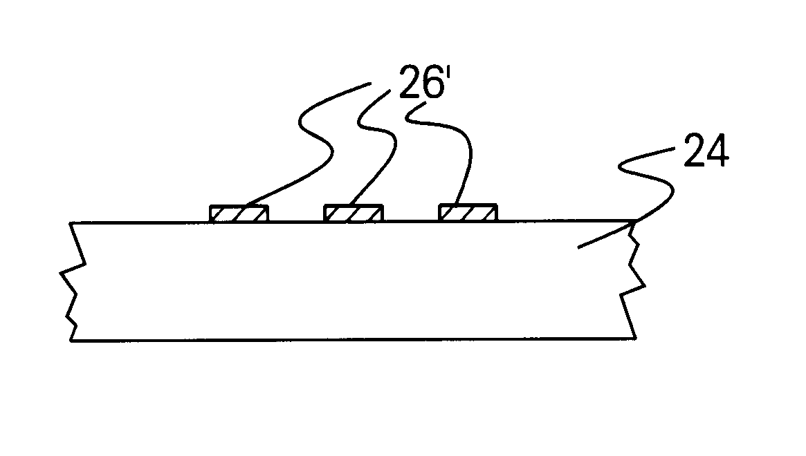
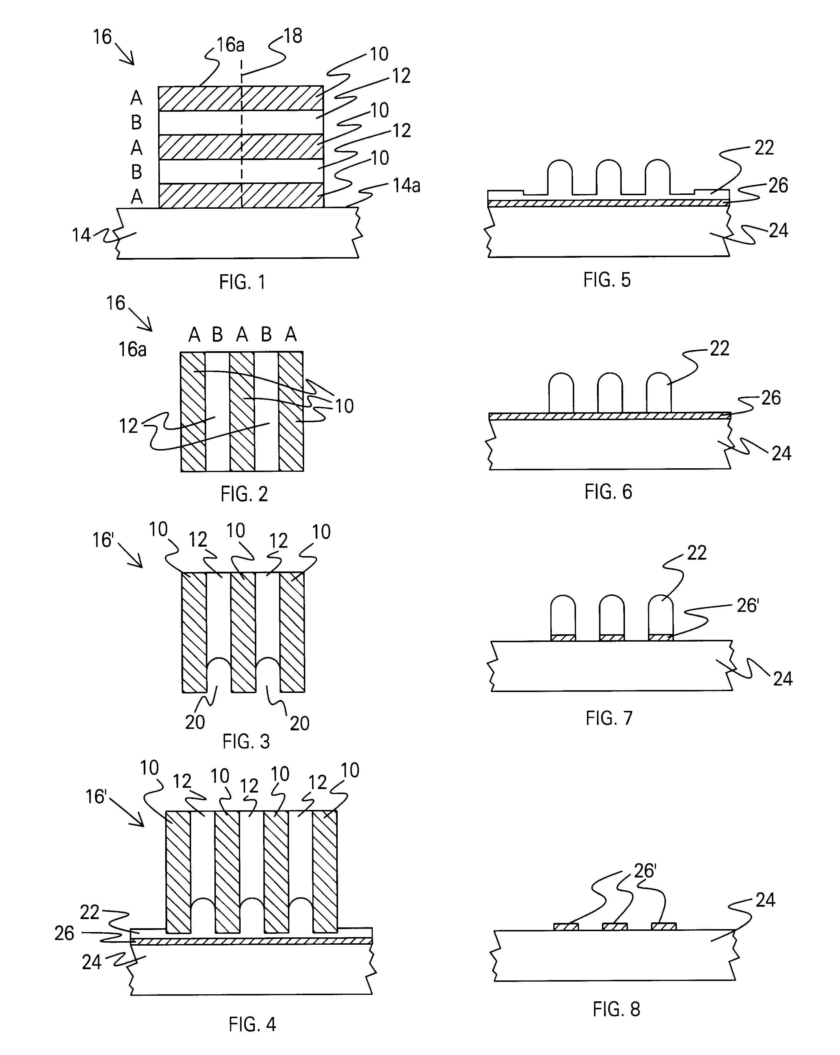
Nanoscale strips for device applications are fabricated by depositing composite thin films with different materials A and B, as illustrated in FIG. 1. Essentially, as described in greater detail below, a plurality of alternating layers of A material 10 and B material 12 are deposited on a major surface 14a of a substrate 14 to form a stack 16, also having a major surface 16a, parallel to the major surface of the substrate. Preferably, the material having the least lattice mis-match with the substrate 14 is deposited in order to keep a smooth growth surface and flat, sharp interfaces between materials 10 and 12.

The layers 10, 12 are then cleaved along a line 18 normal to the major surface 16a of the stack 16 to expose the cross-section, as shown in FIG. 2. Cleaving is performed by any conventional technique useful in cleaving a plurality of alternating layers of dissimilar materials. Such techniques are well-known in the art for the materials used for layers A and B, which are discus...


PUM


Abstract

A method for forming a platen useful for forming nanoscale wires for device applications comprises: (a) providing a substrate having a major surface; (b) forming a plurality of alternating layers of two dissimilar materials on the substrate to form a stack having a major surface parallel to that of the substrate; (c) cleaving the stack normal to its major surface to expose the plurality of alternating layers; and (d) etching the exposed plurality of alternating layers to a chosen depth using an etchant that etches one material at a different rate than the other material to thereby provide the surface with extensive strips of indentations and form the platen useful for molding masters for nano-imprinting technology. The pattern of the platen is then imprinted into a substrate comprising a softer material to form a negative of the pattern, which is then used in further processing to form nanowires. The nanoscale platen thus comprises a plurality of alternating layers of the two dissimilar materials, with the layers of one material etched relative the layers of the other material to form indentations of the one material. The platen is then oriented such that the indentations are parallel to a surface to be imprinted.

Description

With the constantly decreasing feature sizes of integrated-circuit devices, the need for increasingly fine, lithographically-defined patterning is limiting further advances of the technology. Consequently, a growing amount of effort is being devoted to self-assembly techniques to form nanoscale switching elements; see, e.g., C. P. Collier et al, "Electronically Configurable Molecular-Based Logic Gates", Science, Vol. 285, pp. 391-394 (Jul. 16, 1999). The self-assembled switching elements may be integrated on top of a Si integrated circuit so that they can be driven by conventional Si electronics in the underlying substrate. To address the switching elements, nanoscale interconnections or wires, with widths less than 10 .mu.m and lengths exceeding 1 .mu.m, are needed. The self-assembled wires connecting the conventional electronics to the self-assembled switching elements should be anchored at locations defined by the underlying circuitry and should be composed of materials compatibl...

Claims


Application Information

Patent Timeline
IPC IPC(8): H01L21/02H01L21/768H01L21/70H01L21/3213B82B3/00G03F7/00
CPCB82Y10/00B82Y40/00H01L21/3213H01L21/76838G03F7/0002Y10S977/887H01L21/02603H01L21/02532H01L21/02546H01L21/0262H01L21/02631
Inventor CHEN, YONGWILLIAMS, R. STANLEY
Owner SAMSUNG ELECTRONICS CO LTD
Why Eureka
Try Eureka