

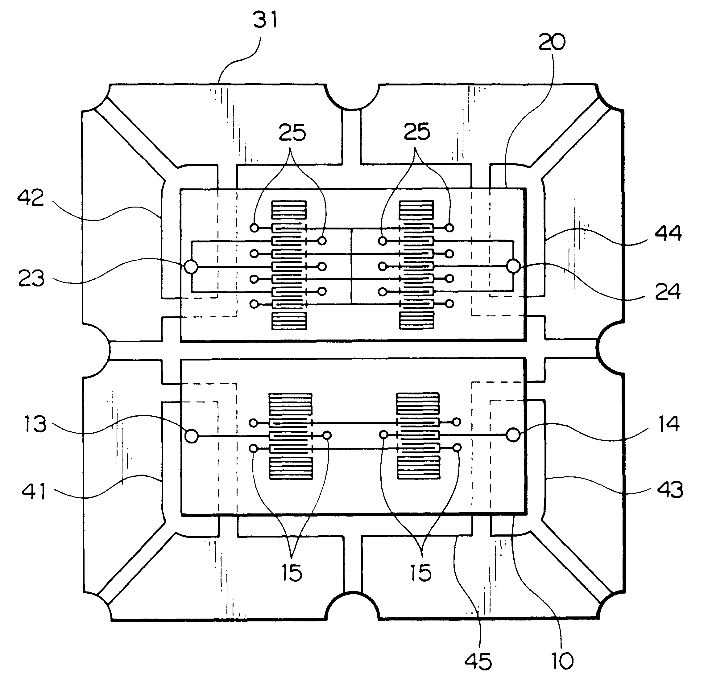
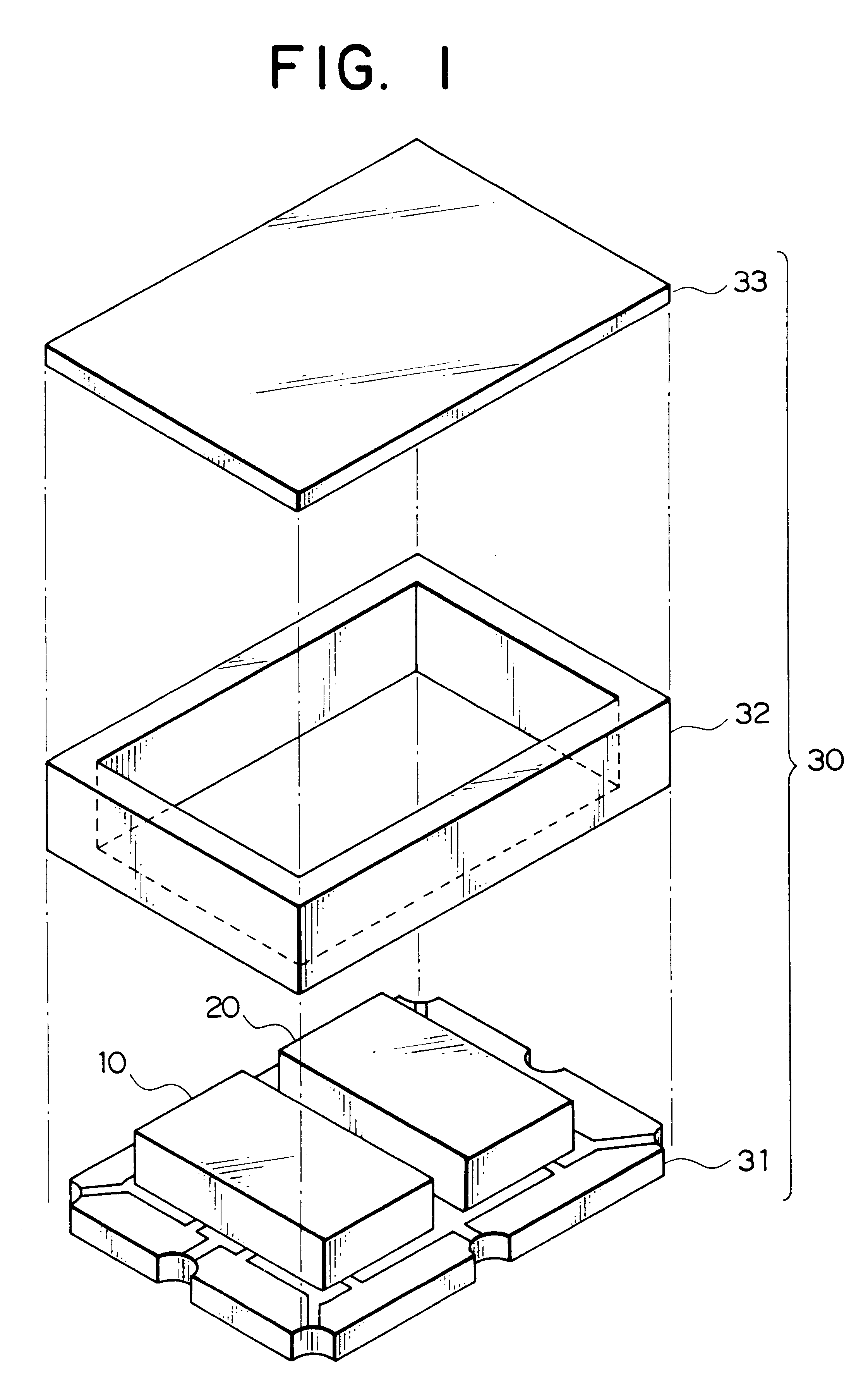
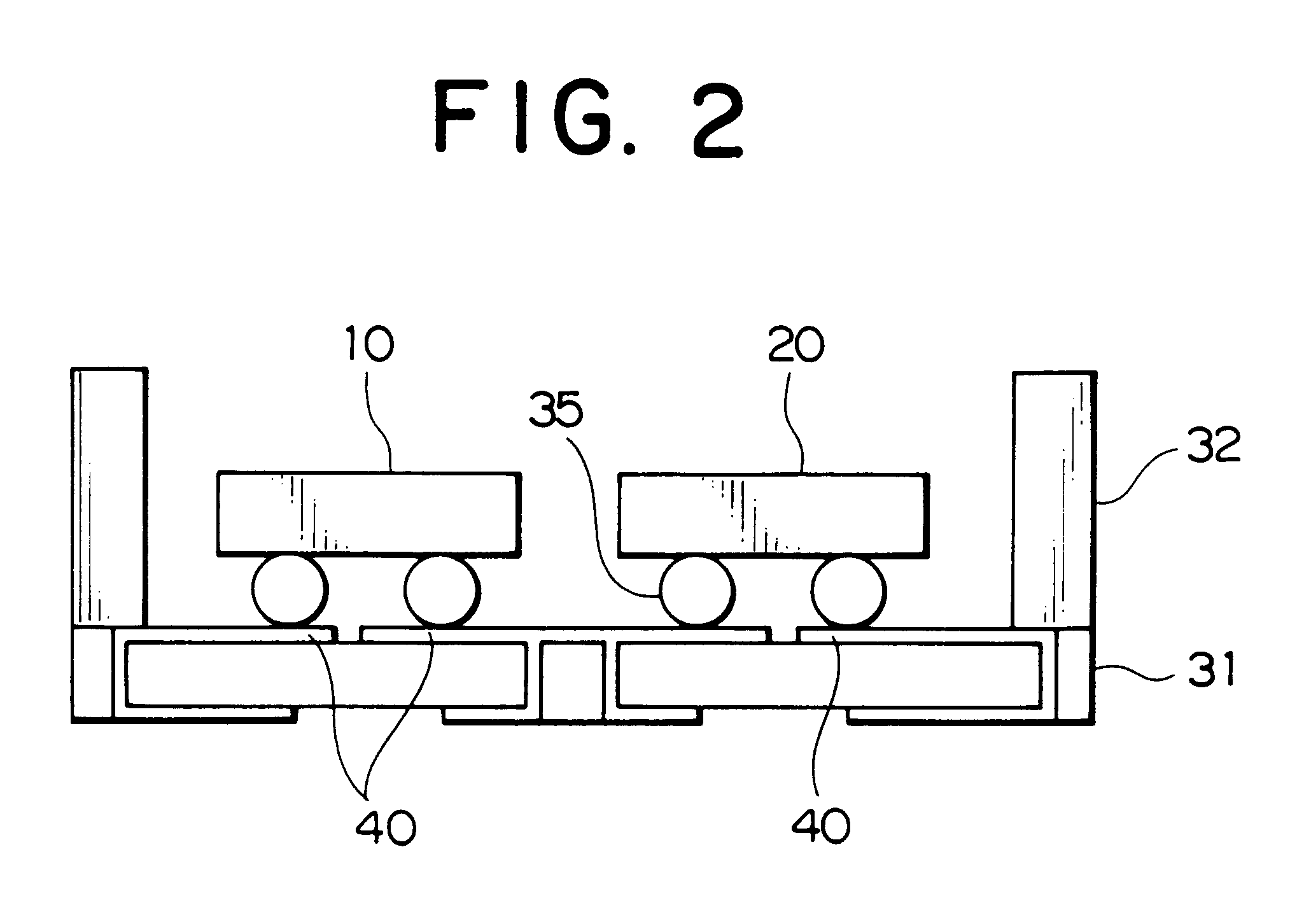
Surface acoustic wave device comprising first and second chips face down bonded to a common package ground
a surface acoustic wave and chip technology, applied in piezoelectric/electrostrictive/magnetostrictive devices, semiconductor devices, piezoelectric/electrostriction/magnetostriction machines, etc., can solve problems such as bump connection and difficulty in adjusting frequency characteristics
- Summary
- Abstract
- Description
- Claims
- Application Information
AI Technical Summary
Benefits of technology
Problems solved by technology
Method used
Image

Examples
Embodiment Construction
Embodiment of the present invention is not restricted to the aforementioned embodiments. As long as being within the range of the technical idea of the present invention, it can be extended and modified. These extended or modified embodiments are also included in the present invention.
As examples of extension and modification, the following can be cited.
(1) Though two chips are used to constitute a surface acoustic wave device in the above embodiments, three or more chips can be used to constitute.
In this case too, all of the IDTs on the respective chips is preferable to face the ground conductor 45 on the base 31 so as to prevent signals and noise from mingling.
Further, on the area between signal conductors 41 to 44 on the base 31 part of the ground conductor 45 is preferable to exist. Furthermore, the signal conductors 41 to 44, except for one side or one edge thereof, are preferable to be surrounded in a state adjacent to the ground conductor 45.
(2) When surface acoustic wave chi...
PUM
 Abstract
Description
Claims
Application Information