Image forming apparatus and exposure device thereof
a technology of exposure device and image forming apparatus, which is applied in the direction of inking apparatus, instruments, electrographic processes, etc., can solve the problems of deterioration of the quality of printed images, difficulty in wire-ball-free connection,
- Summary
- Abstract
- Description
- Claims
- Application Information
AI Technical Summary
Problems solved by technology
Method used
Image
Examples
first embodiment
(B) Modification of First Embodiment
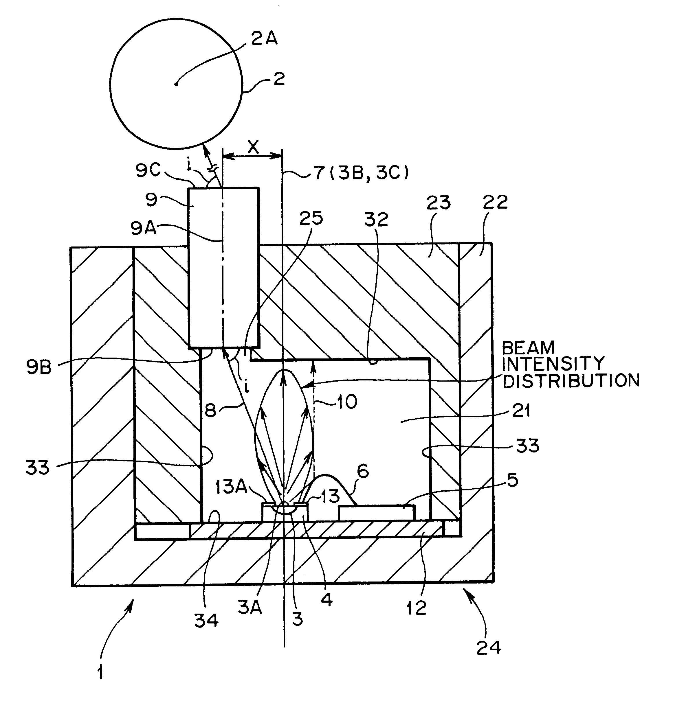
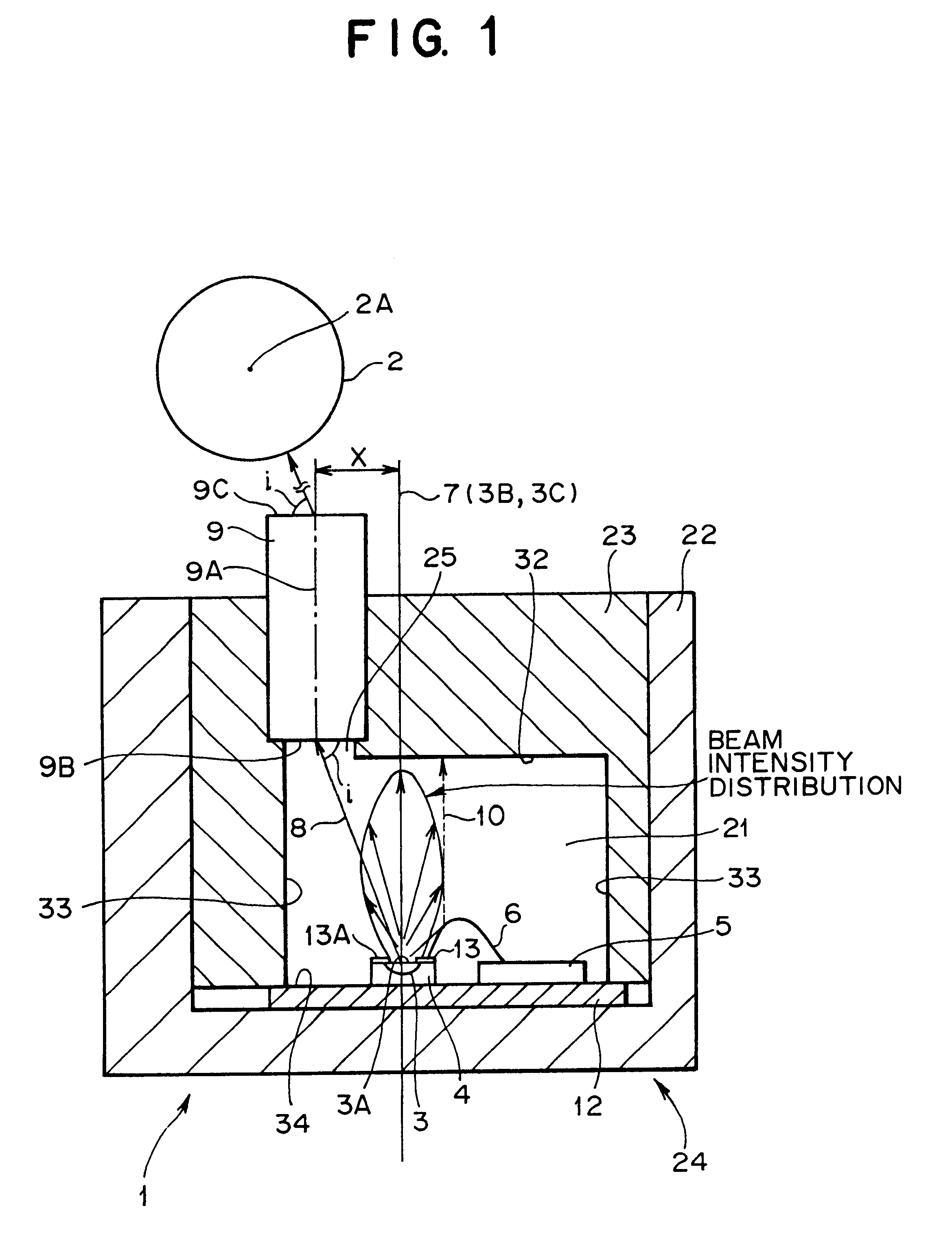
FIG. 5 shows a cross-sectional view showing a modification of the exposure device 1 of the first embodiment. This modified exposure device 1B comprises an exposure body 24B, which is a substitute for the exposure body 24 of the first embodiment.
Like reference numbers designate similar parts or elements throughout several views of different illustrated examples, so any repetitious description is omitted here.
The exposure body 24B, as shown in FIG. 5, is composed of an outer casing 22B and an inner casing 23B, which are generally C-shaped in cross section, the inner casing 23B being telescopically fitted in the outer casing 22B with their through-hole sides facing each other. As a significant feature, the inner casing 23B has a non-uniform-thickness horizontal wall increasing gradually from one side to the other. With this arrangement, a light-emitting space 21B is defined inside the exposure body 24B as surrounded by a top wall (hereinafter called ...
second embodiment
(C) Description of Second Embodiment
FIG. 6 shows a cross-sectional view schematically showing another exposure device according to a second embodiment of the present invention. The exposure device 1C of the second embodiment comprises an exposure body 24C, which is a substitute for the exposure body 24 of the first embodiment.
Like reference numbers designate similar parts or elements throughout several views of different illustrated examples, so any repetitious description is omitted here.
The exposure body 24C, as shown in FIG. 6, is composed of an outer casing 22C and an inner casing 23C, which are generally C-shaped in cross section, the inner casing 23C being telescopically fitted in the outer casing 22B with their through-hole sides facing each other. As a significant feature, the inner casing 23C has a non-uniform-thickness side wall inclined with respect to the bottom. With this arrangement, a light-emitting space 21C is defined inside the exposure body 24C as surrounded by a ...
third embodiment
(D) Description of Third Embodiment
FIG. 7 shows a cross-sectional view schematically showing another exposure device according to a third embodiment of the present invention. The exposure device 1D of the third embodiment comprises an exposure body 24D, which is a substitute for the exposure body 24 of the first embodiment.
Like reference numbers designate similar parts or elements throughout several views of different illustrated examples, so any repetitious description is omitted here.
In the third embodiment, a plurality of driver elements 5 are disposed on both side of the LED array 4 on the print board 12 in series parallel to the LED array 4, and the LED array 4 and the associated driver elements 5 of each set are interconnected via wires 61 with wire balls.
The individual wire 61 has a wire ball 11 at at least one end. The driver element 5, on the right side of the LED microchip 4 in FIG. 7 is connected to the mask 13 on the surface of the LED array 4. The mask 13 is connected t...
PUM
 Abstract
Description
Claims
Application Information


