Configurable integrated circuit and method of testing the same

a technology of integrated circuits and integrated circuits, applied in the direction of electronic circuit testing, measurement devices, instruments, etc., can solve the problems of low packaging density, slow operation speed, and never been used

Inactive Publication Date: 2002-02-19
KK TOSHIBA
View PDF10 Cites 44 Cited by
  • Summary
  • Abstract
  • Description
  • Claims
  • Application Information

AI Technical Summary

Problems solved by technology

The integrated circuits having CLBs, however, involve low packaging density and slow operation speed.
Accordingly, they have never been used in fields where high packaging density and high operation speed are important.
Due to these problems, it is difficult to apply CLBs to fields where packaging density and operation speed are important.
Another problem of CLBs is difficulty in testing them because they are configurable. FIG. 1B shows a method of testing a CLB according to a prior art.
These factors complicate the testing of CLBs.

Method used


Image

  • Configurable integrated circuit and method of testing the same
  • Configurable integrated circuit and method of testing the same
  • Configurable integrated circuit and method of testing the same

Examples


first embodiment

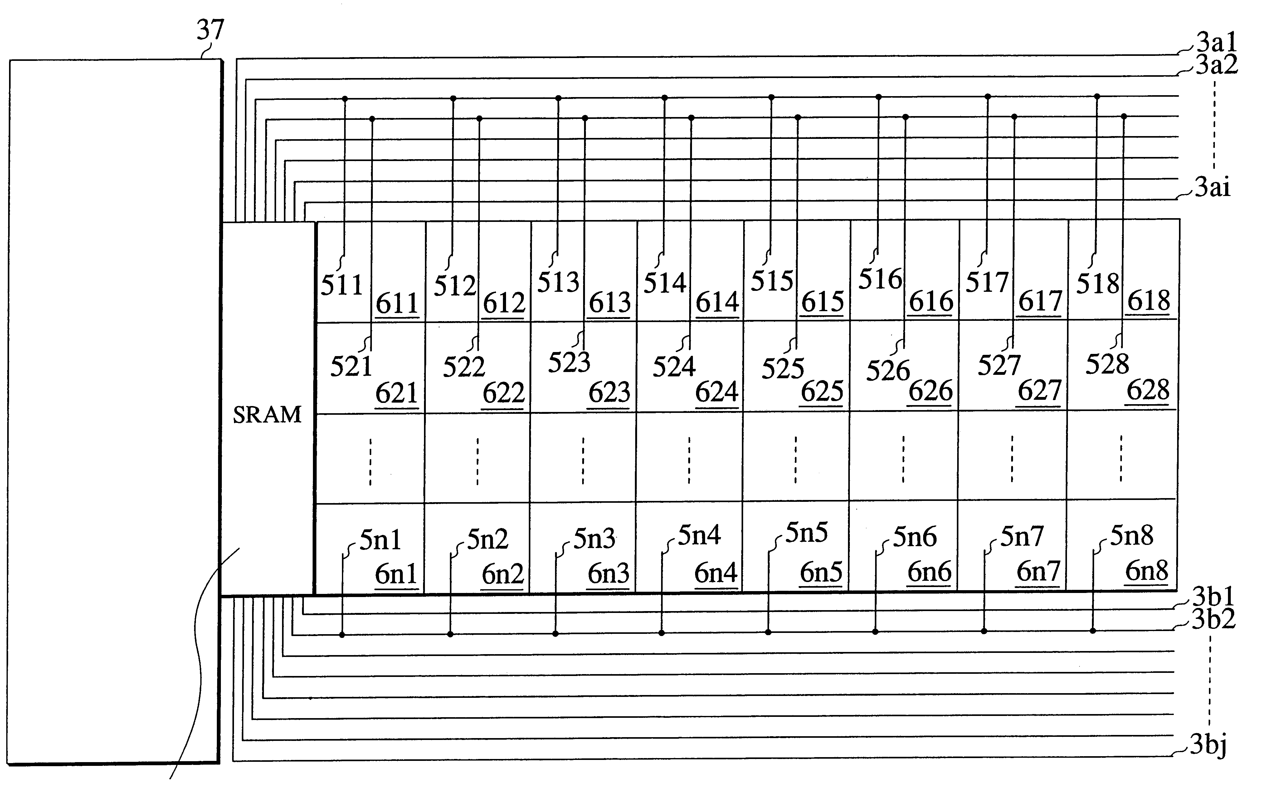
The first embodiment supplies the same configuration data from the SRAM 31 to eight CLBs such as the CLBs 611 to 618. This reduces the number of memories and an area occupied by memories to one eighth of the prior art.

If the ratio of an area occupied by operational elements such as multiplexers and inverters to an area occupied by an SRAM in an integrated circuit is 50:50, the first embodiment reduces the SRAM area to one eighth of the prior art and the total of the element area and SRAM area to 56% of the prior art.

Although not shown, the integrated circuit of FIG. 3 has registers for storing data to process and results of intermediate operations and data lines for connecting the registers to the operational elements.

second embodiment

FIG. 4 shows an integrated circuit according to the present invention. The integrated circuit has configurable logic blocks (CLBs) 611 to 6k8, hard-wired logic blocks (HLBs) 911 to 9f8, an SRAM 312, and a controller 372. The SRAM 312 stores configuration data for configuring the CLBs and block-connection data for determining connections among the CLBs and HLBs.

The HLBs 911 to 9f8 have fixed functions. Unlike the CLBs, the HLBs are unable to change their functions according to configuration data. For example, an HLB to which an exclusive OR function is assigned serves only as an exclusive OR logic block.

It is possible, however, to change connections between the HLBs, between the CLBs, and between the CLBs and the HLBs. For example, the output of the HLB 911 is connected to an input of the CLB 6k1, and the output of the CLB 6k1 to an input of the HLB 9f1. Without using the CLB, it is possible to connect the output of the HLB 911 to an input of the HLB 9f1.

Operations carried out by the...

third embodiment

FIG. 5 shows an integrated circuit according to the present invention. The integrated circuit has CLBs C1-611 to C8-6k8, HLBs C1-911 to C8-9f8, an SRAM 313, and a controller 373. The SRAM 313 stores configuration data for configuring the CLBs, and block-connection data for determining connections among the CLBs and HLBs. The SRAM 313 or the controller 373 stores partial-circuit-connection data for determining connections between partial circuits consisting of logic blocks.

Operations carried out by the CLBs may be taken over by HLBs. If possible, all operations may be executed by HLBs. Namely, the CLBs may partly or entirely be replaced with HLBs.

The size of HLB may be as small as an AND circuit, intermediate-sized like an Adder circuit, or as large as an Arithmetic and Logic Unit.

Under the control of the controller 373, the block-connection data configures connections between the CLBs, between the HLBs, and between the CLBs and the HLBs. For example, a partial circuit C1 for carryin...


PUM


Abstract

An integrated circuit has configurable logic blocks that are reconfigurable, hard-wired logic blocks that carry out fixed operations, and a memory. The memory stores configuration data for configuring the configurable logic blocks, block-connection data for determining connections between the configurable and hard-wired logic blocks, and partial-circuit-connection data for determining connections between partial circuits each of which consists of logic blocks selected among the configurable and hard-wired logic blocks. These pieces of data are shared by the logic blocks to reduce the number of memories in the integrated circuit and improve the packaging density of the integrated circuit.

Description

1. Field of the InventionThe present invention relates to an integrated circuit and a method of testing the same. In particular, the present invention relates to an integrated circuit having configurable logic blocks (CLBs) that are configurable according to external signals and a method of testing such an integrated circuit.2. Description of the Related ArtIntegrated circuits having CLBs that are configurable according to external signals are flexible to use, and therefore, their demand is increasing.The integrated circuits having CLBs, however, involve low packaging density and slow operation speed. Accordingly, they have never been used in fields where high packaging density and high operation speed are important.FIG. 1A roughly shows a CLB 1 and a CLB memory 3 according to a prior art. The CLB memory 3 stores data for configuring the CLB 1. The prior art provides each CLB with a CLB memory. If many CLBs each having a CLB memory are installed in an integrated circuit, the CLB mem...

Claims


Application Information

Patent Timeline
Patent Type & Authority Patents(United States)
IPC IPC(8): G01R31/28G01R31/3185
CPCG01R31/318516
Inventor OHUCHI, KAZUNORIYOSHIDA, MASAKOOOWAKI, YUKIHITOFUJII, HIROSHIGESEKINE, MASATOSHI
Owner KK TOSHIBA
Why Eureka
Try Eureka