Thin film semiconductor device and method for producing the same

a thin film semiconductor and semiconductor technology, applied in non-linear optics, instruments, coatings, etc., can solve the problems of increasing display size, slow operating speed, and inferior electrical characteristics of polysilicon layers

Inactive Publication Date: 2002-05-21
SEIKO EPSON CORP
View PDF35 Cites 76 Cited by
  • Summary
  • Abstract
  • Description
  • Claims
  • Application Information

AI Technical Summary

Problems solved by technology

The previously mentioned amorphous silicon layers, however, have such problems as electrical characteristics far inferior to those of polysilicon layers and slow operating speed.
Since the high temperature process polysilicon TFTs use quartz substrates, however, there are problems with increasing display size and increasing costs.
But, when using large substrates which are well-suited to mass production, there is a severe restriction in that the substrates must be kept below a maximum processing temperature of about 400.degree. C. in order to avoid substrate deformation.
Conversely, if the energy intensity is strong, the Si film is damaged and the PECVD a-Si film again does not crystallize at all.
As described above, however, there are several inherent problems with poly-Si TFTs fabricated by each of the existing technologies in the prior art of the low temperature process which act as impediments to the adoption of these technologies into mass production.
Problems associated with the first type of prior art.
The high processing temperature of 550.degree. C. prevents the use of low-priced glass leading to a steep rise in product prices.
Additionally, the degree of warp of the glass substrates as a result of their own weight increases as substrate size increases, and increases in liquid crystal display (LCD) sizes are not possible.
There is a thought to move from the present 360 mm.times.460 mm glass substrates for LCDs to larger 550 mm.times.650 mm substrates, but there are no LPCVD reactors which can accommodate the increase in substrate size.
Problems associated with the second type of prior art.
Accompanying this, it becomes impossible to use low-priced glass leading to a steep rise in product prices.
Additionally, the degree of warp of the glass substrates as a result of their own weight increases as substrate size increases, and increases in liquid crystal display (LCD) sizes are not possible.
Conversely, with the use of a low annealing temperature less than about 450.degree. C., the degree of crystallization from the laser irradiation can vary from uniform to non-uniform from lot to lot and reliable production is not possible.
If the degree of crystallization is low, a good quality crystalline semiconductor film cannot be obtained.
For this reason, the second type of prior art is comparatively more expensive than the first type of prior art.
Also, as the process becomes longer, the product yield decreases.
Additionally, as for the case in 1-2 above, there are no furnaces available which can accommodate increases in substrate size.
Problems associated with the third type of prior art.
As a result, the productivity decreases noticeably, receding to a steep rise in product prices.
Consequently, in the third type of prior art, if the laser irradiation is not performed in vacuum or a nonoxygen atmosphere, it is not possible to obtain semiconductor films without oxygen.
This means further decreases in productivity and further increases in product prices.
Therefore, a good quality semiconductor cannot be obtained even if there is no oxygen incorporation; and the characteristics of a thin film semiconductor device using this type of film will not be good.
On the other hand, when an amorphous silicon film is used as the active layer in a thin film semiconductor device (hereafter abbreviated as a-Si TFT), the mobility is on the order of 0.1 cm.sup.2.times.V.sup.-1.times.sec.sup.-1 ; and a problem arises in that the response speed is too slow for switching elements in a high-precision color LCD having, for example, 768 (rows).times.1024 (columns).times.3 (colors).times.2359296 (pixels), and the TFTs cannot be used.
Also, since preheating chambers are indispensable in the deposition method using single substrate PECVD reactors, a problem arises in that increases in PECVD reactor size lead to steep increases in price.
After the substrates are set in the reaction chamber, a long preheat is still necessary; and this is one cause of decreased productivity.

Method used


Image

  • Thin film semiconductor device and method for producing the same
  • Thin film semiconductor device and method for producing the same
  • Thin film semiconductor device and method for producing the same

Examples


example 1

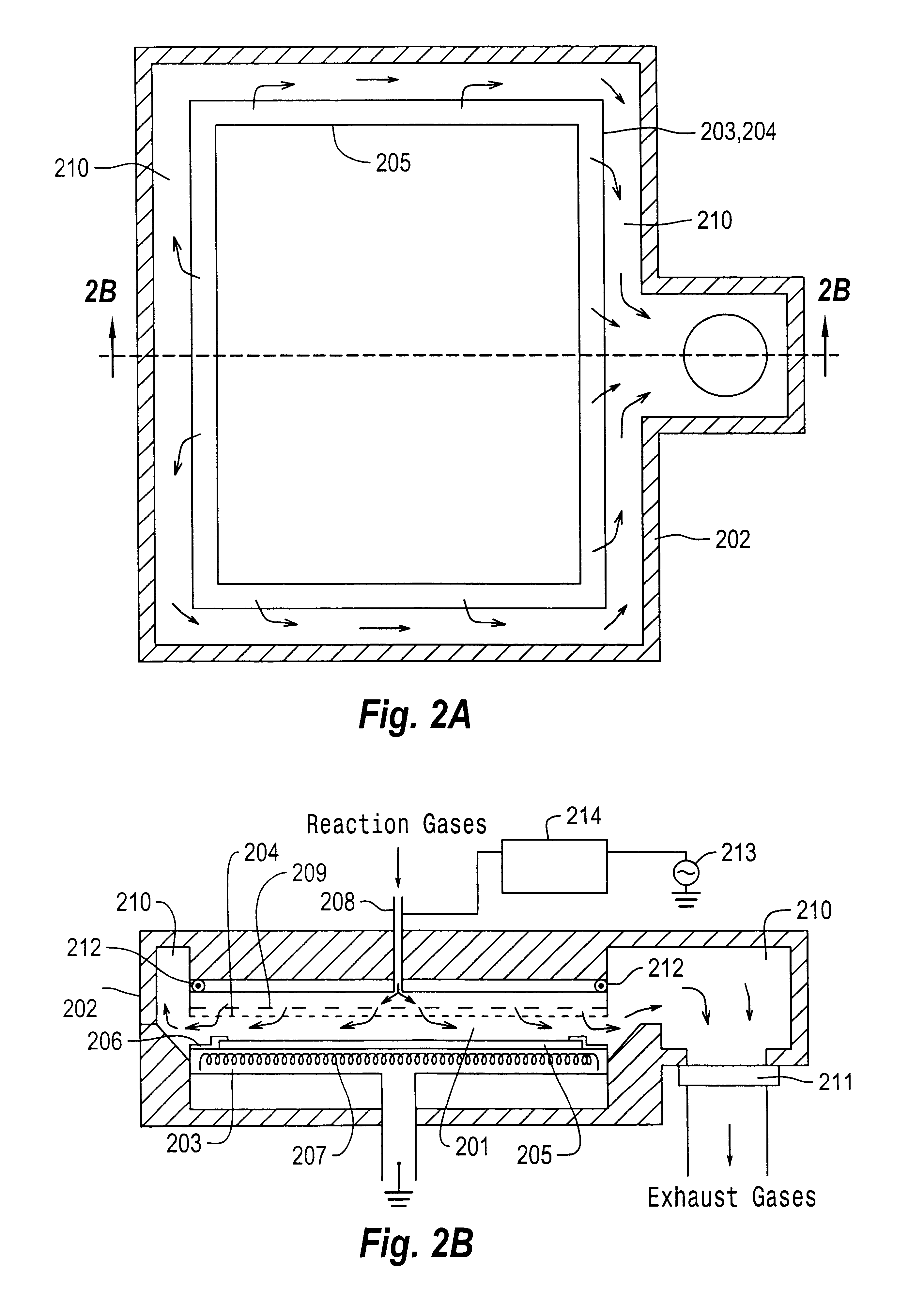
An example of a semiconductor film according to the present invention and its fabrication by PECVD will be explained. After forming an underlevel protection layer, consisting of an insulating material such as a silicon oxide film, on at least part of the surface of a substrate, a semiconductor film is formed over this underlevel protection layer using the PECVD reactor described in detail in section (2-3).

A 360 mm.times.475 mm.times.1.1 mm glass substrate (OA-2) which is at room temperature is set in the PECVD reactor, the lower plate electrode 203 of which is maintained at a temperature of 380.degree. C. The recipe followed once the substrate is in place in the PECVD reaction furnace is as follows.

(Preheat 1)

Time: t=90 s

Hydrogen flow rate: H.sub.2 =100 SCCM

Helium flow rate: He=3000 SCCM

High frequency power: RF=0 W (no plasma)

Pressure: P-3.0 Torr

Electrode separation: S=37.1 mm

Lower plate electrode temperature: Tsus=380.degree. C.

(Preheat 2)

Time: t=60 s

Silane flow rate: SiH.sub.4 =10...

example 2

A thin film semiconductor device was fabricated using the as-deposited semiconductor film obtained as described in Example 1 as the active layer of a TFT.

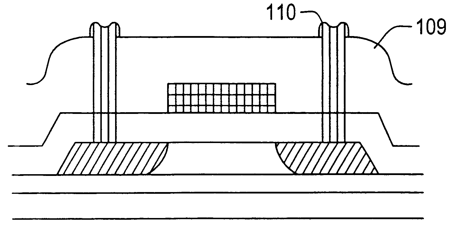
First, underlevel protection layer 102, which consists of a silicon oxide film, is formed on substrate 101 by PECVD. Then, without breaking the vacuum, an intrinsic silicon layer which becomes the active layer of the thin film semiconductor device is sequentially deposited over this underlevel protection layer using the method described in Example 1. The thickness of the underlevel protection layer is 300 nm and the thickness of the semiconductor film is 90 nm. Accordingly, the semiconductor film deposition time is 247 seconds. Semiconductor films obtained in this way can be used in the as-deposited state as the active layer which serves, for example, as the channel region of the TFT.

After the substrate is removed from the PECVD reactor, these microconductor film is patterned and thin film layer 103, which later becomes the active ...

example 3

An active matrix substrate was fabricated using the thin film semiconductor devices obtained in Example 2 as the pixel switching elements for a high-definition color LCD which was comprised of 768 (rows).times.1024 (columns).times.3 (colors)=2359296 pixels. As in Example 2, the source electrode and source interconnects in Example 3 are aluminum; the drain electrodes, however, are indium tin oxide (ITO). A liquid crystal panel was manufactured that employed an active matrix substrate obtained in this way for one of the two substrates in the substrate pair. A liquid crystal display device was produced by assembling the liquid crystal panel thus obtained together with external peripheral driving circuits and a backlight unit. Because the TFTs are high performance and the parasitic capacitance of the transistors is extremely small, a high aperture ratio, bright, high-quality liquid crystal display device was obtained. In addition, because the fabrication process for the active matrix su...


PUM

PropertyMeasurementUnit
pressureaaaaaaaaaa
deposition rateaaaaaaaaaa
temperatureaaaaaaaaaa

Abstract

In order to fabricate a high performance thin film semiconductor device using a temperature process in which it is possible to use inexpensive glass substrates, a highly crystalline mixed-crystallinity semiconductor film is deposited by means of PECVD using a silane as the source gas and argon as the dilution gas, then the crystallinity of this film is improved by such means as laser irradiation. Thin film semiconductor devices fabricated in this way are used in the manufacture of such things as liquid crystal displays and electronic devices.In applying the present invention to the fabrication of an active matrix liquid crystal display, it is possible to both easily and reliably fabricate a large, high-quality liquid crystal display. Additionally, in applying the present invention to the fabrication of other electronic circuits as well, it is possible to both easily and reliably fabricate high-quality electronic circuits.

Description

FIELD OF TECHNOLOGYThe present invention relates first of all to thin film semiconductor devices, and the fabrication methods for such devices, which are suitable for active matrix liquid crystal displays and the like. The present invention also relates to liquid crystal displays for which the thin film semiconductor devices are appropriate, the fabrication processes for such liquid crystal displays, electronic devices, and the fabrication processes for such electronic devices. Further, the present invention relates to thin film deposition processes using plasma-enhanced chemical vapor deposition (PECVD).BACKGROUND TECHNOLOGYIn recent years, along with increases in screen size and improvements in resolution, the driving methods for liquid crystal displays (LCDS) are moving from simple matrix methods to active matrix methods; and the displays are becoming capable of displaying large amounts of information. LCDs with more than several tens of thousands pixels are possible with active ...

Claims


Application Information

Patent Timeline
Patent Type & Authority Patents(United States)
IPC IPC(8): C23C16/02C23C16/22C23C16/24H01L21/02H01L21/205H01L21/336G02F1/13G02F1/1362H01L21/20H01L21/285H01L29/786
CPCC23C16/0209C23C16/0272C23C16/24H01L21/28525H01L29/66757H01L21/0262H01L29/78675H01L21/0237H01L21/02532H01L21/02576H01L21/02579H01L29/78609G02F1/13454
Inventor MIYASAKA, MITSUTOSHI
Owner SEIKO EPSON CORP
Why Eureka
Try Eureka