Polishing process monitoring method and apparatus, its endpoint detection method, and polishing machine using same

a technology of polishing process and monitoring method, which is applied in the direction of lapping machines, instruments, manufacturing tools, etc., can solve the problems of inability to detect inability to monitor the polishing process correctly, and difficulty in detecting the endpoint of the polishing process

Inactive Publication Date: 2002-07-30
NEC CORP
View PDF7 Cites 44 Cited by
  • Summary
  • Abstract
  • Description
  • Claims
  • Application Information

AI Technical Summary

Problems solved by technology

If the degree of polishing is insufficient, in other words, the polishing operation is stopped prematurely, the metal layer tends to be partially left on the underlying dielectric layer, causing electrical short circuit between the wiring lines and / or contact plugs.
With the prior-art in-situ monitoring apparatus shown in FIG. 1, however, there is a problem that the polishing process may be unable to be monitored correctly according to the material of the semiconductor wafer 101, the thickness of the layered structure on the wafer 101, or the pattern (i.e., geometry or closeness / coarseness) of the wiring lines and / or contact plugs.
As a result, the endpoint of the polishing process is very difficult or unable to be detected correctly.
However, the nozzle may be omitted if the rotation speed of the wafer is high enough for the slurry to be fully spread and to be sufficiently thin on the whole wafer due to the centrifugal force, applying no effect to detection of the specular-reflected light beam.

Method used


Image

  • Polishing process monitoring method and apparatus, its endpoint detection method, and polishing machine using same
  • Polishing process monitoring method and apparatus, its endpoint detection method, and polishing machine using same
  • Polishing process monitoring method and apparatus, its endpoint detection method, and polishing machine using same

Examples


first embodiment

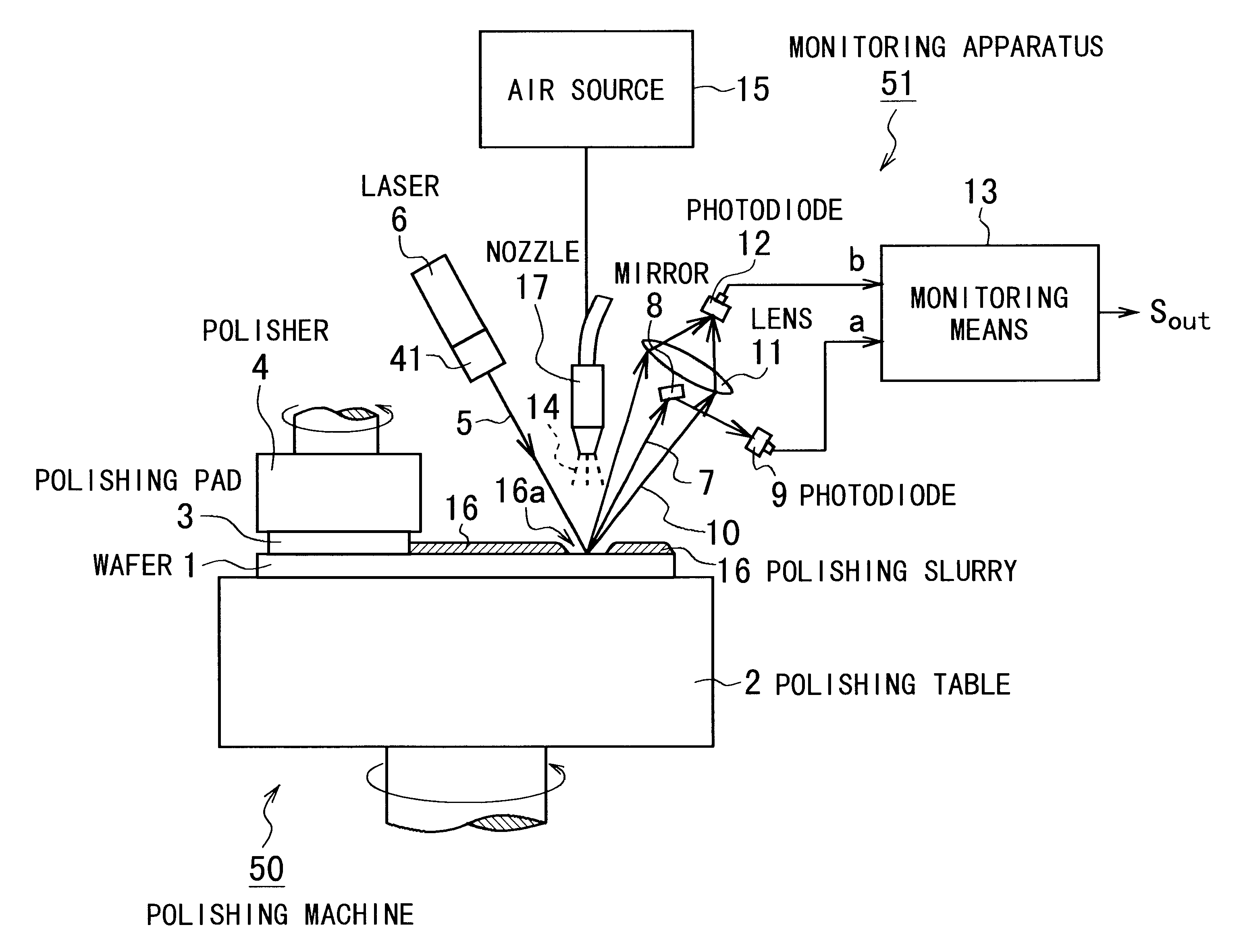
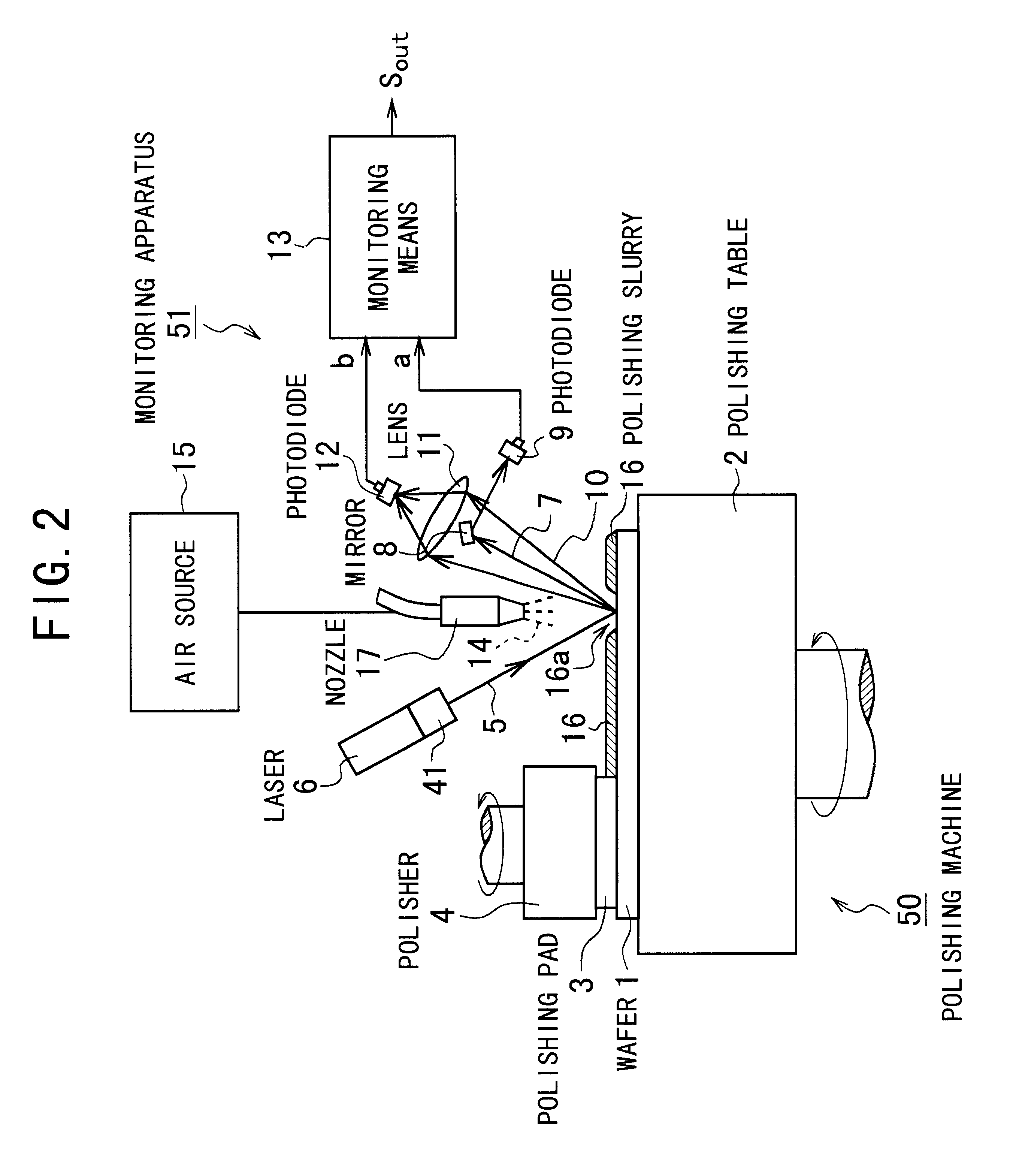
As shown in FIG. 2, a polishing machine 50 is equipped with a circular polishing table 2, a polisher 4, and a monitoring apparatus 51 according to the present invention. This machine 50 is used to carry out a CMP process of a semiconductor wafer 1.

The table 2, which is rotatable in a horizontal plane around a vertical axis, holes a semiconductor wafer 1 on its top face. The wafer 1 held on the top face of the table 2 is rotated along with the table 2 on operation. The polisher 4 is rotatable in a horizontal plane around a vertical axis and is slidable off the same vertical axis in the same horizontal plane. The polisher has a polishing pad 3 attached onto its bottom face. On operation, the pad 3 on the rotating polisher 4 is contacted with the upper surface (i.e., the polishing surface) of the wafer 1 under a specific pressure while being moved along the surface of the wafer 1.

The monitoring apparatus 51, which monitors in situ the polishing process or polished state of the wafer 1,...

second embodiment

FIG. 4 shows a polishing machine 50A equipped with a monitoring apparatus 51A according to a second embodiment of the present invention, which is comprised of the same polishing mechanism as that of the polishing machine 50 of FIG. 2. However, it has the monitoring apparatus 51A instead of the monitoring apparatus 51 according to the first embodiment of FIG. 2.

The monitoring apparatus 51A has the same configuration and operation as those of the monitoring apparatus 51 except that the specular-reflected light beam 7 generated from the detection light beam 5 is directly received by a photodiode 44. The photodiode 44 is located on the optical axis of the beam 7 at the near-side of the condensing lens 11. The photodiode 44 receives directly the specular-reflected light beam 7 and measures its amount, outputting a first electric signal a according to the measured amount of the specular-reflected light beam 7 to the monitoring means 13.

The diameter and contour of the light-receiving surfa...

third embodiment

FIG. 5 shows a polishing machine 50B equipped with a monitoring apparatus 51B according to a third embodiment of the present invention, which is comprised of the same polishing mechanism as that of the polishing machine 50 according to the first embodiment of FIG. 2. However, it has a monitoring apparatus 51B instead of the monitoring apparatus 51 according to the first embodiment of FIG. 2.

The monitoring apparatus 51B which monitors in situ the polishing process or polished state of the wafer 1, is comprised of a first photodiode 20, an ellipsoidal mirror 21, a second photodiode 22, and a third photodiode 23.

The first photodiode 20, which is located on the optical axis of the specular-reflected light beam 7, receives directly the specular-reflected light beam 7 and measures its amount, outputting a first electric signal c to the monitoring means 13.

The ellipsoidal mirror 21 is located on the optical axis of the specular-reflected light beam 7 at a position downstream with respect t...


PUM

PropertyMeasurementUnit
reflectionaaaaaaaaaa
thresholdaaaaaaaaaa
threshold valueaaaaaaaaaa

Abstract

A polishing process monitoring apparatus of a semiconductor wafer is provided, which is capable of monitoring correctly the process independent of various factors affecting optical measurement, such as the configuration, material, and size of a layered structure on the wafer, and the geometric shapes of patterns and their arrangement for respective semiconductor chips. This apparatus is comprised of (a) a light irradiating means for irradiating a detection light beam to a semiconductor wafer, (b) a first light receiving means for receiving a specular-reflected light beam generated by reflection of the detection light beam at the wafer and for outputting a first signal according to an amount of the specular-reflected light beam, (c) a second light receiving means for receiving a scattered / diffracted light beam generated by scattering or diffraction of the detection light beam at the wafer and for outputting a second signal according to an amount of the scattered / diffracted light beam, and (d) a monitoring means for monitoring a polishing process of the wafer by using the first and second signals.

Description

1. Field of the InventionThe present invention relates to a method and an apparatus of monitoring a polishing process of a semiconductor wafer, which are suitably applied to the well-known Chemical Mechanical Polishing (CMP) process, a method of detecting an endpoint of the polishing process, and a polishing machine equipped with the monitoring apparatus.2. Description of the Prior ArtTo form wiring or interconnecting lines, contact plugs penetrating via holes, and so on, for electronic devices or elements formed on a semiconductor wafer, conventionally, the so-called CMP process has been used. In this case, typically, a dielectric layer is formed on or over the entire wafer to cover the electronic devices or elements and then, a metal layer is formed to overlay the whole dielectric layer. Subsequently, an upper, unnecessary part of the metal layer is globally polished away by a polishing machine until the remaining metal layer has a desired pattern designed for the wiring lines, co...

Claims


Application Information

Patent Timeline
Patent Type & Authority Patents(United States)
IPC IPC(8): B24B37/04B24B49/04B24B49/02B24B49/12B24B37/013B24B1/00H01L21/304
CPCB24B37/013B24B37/042B24B49/04B24B49/12B24B1/00
Inventor TAKEISHI, AKIRAMITSUHASHI, HIDEOOHKAWA, KATSUHISAHAYASHI, YOSHIHIROONODERA, TAKAHIRO
Owner NEC CORP
Why Eureka
Try Eureka