Protective plate for a plasma display and a method for producing the same

a technology for protecting plates and plasma displays, applied in the field of protective plates, can solve problems such as high possibility of damag

Inactive Publication Date: 2002-09-17
ASAHI GLASS CO LTD
View PDF20 Cites 48 Cited by
  • Summary
  • Abstract
  • Description
  • Claims
  • Application Information

AI Technical Summary

Problems solved by technology

Since a conventional PDP comprises very precise electric components, if it was used as it is and if a user acted on it to apply a force to its surface, there was a high possibility of causing damage.
Further, since PDP generates electromagnetic waves harmful to human body and near infrared rays which causes erroneous operations of remote controllers for various kinds of electrical equipments, there has raised necessity for providing a protective plate having a shielding property to the electromagnetic waves.

Method used


Image

  • Protective plate for a plasma display and a method for producing the same
  • Protective plate for a plasma display and a method for producing the same
  • Protective plate for a plasma display and a method for producing the same

Examples


example

Example 1

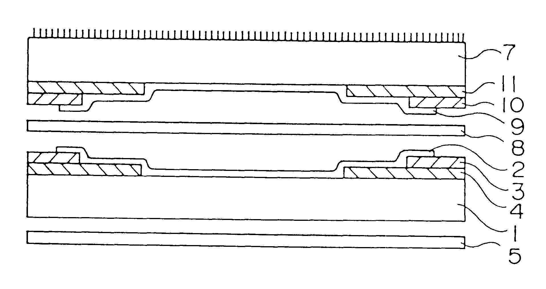
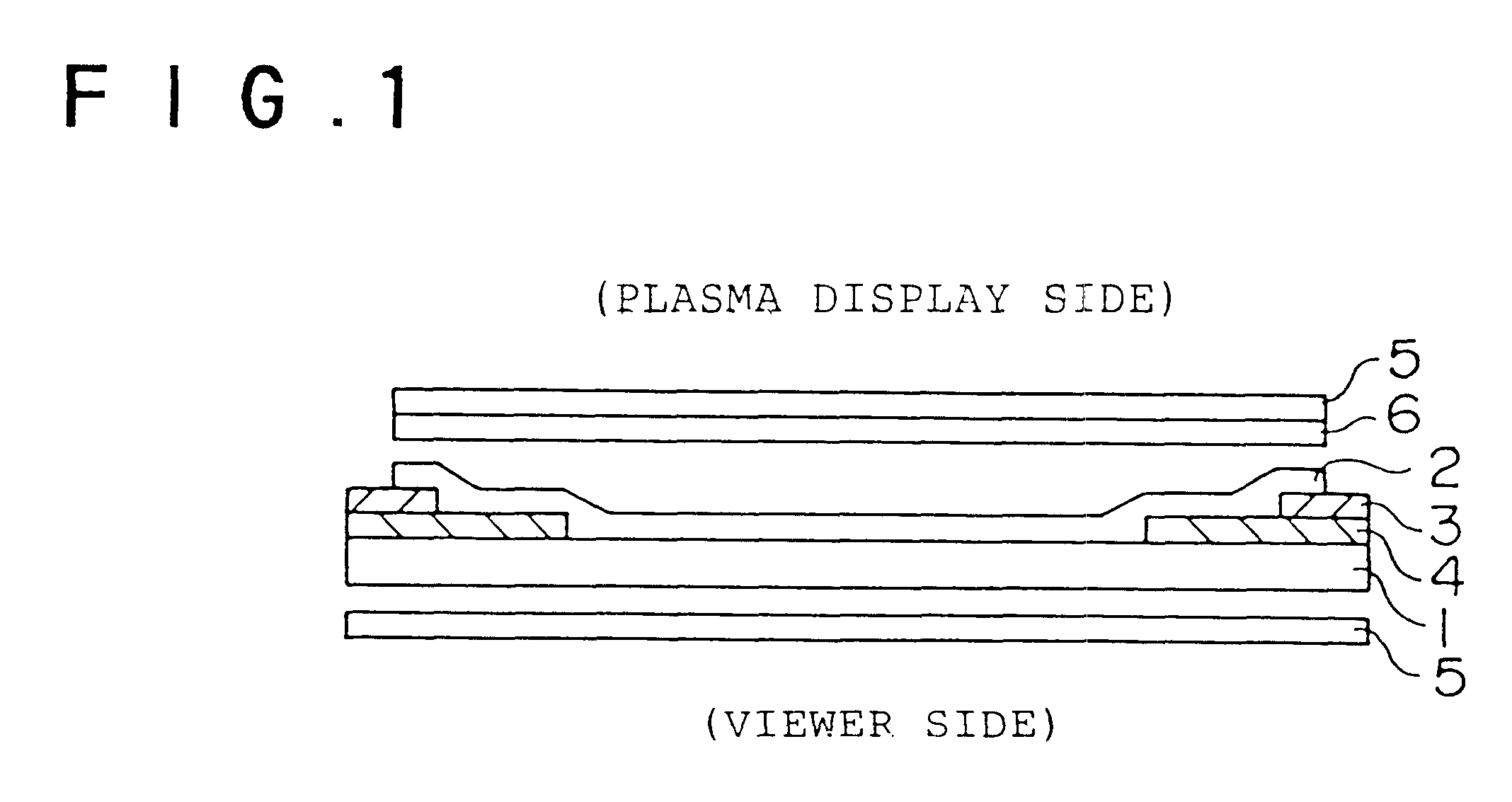
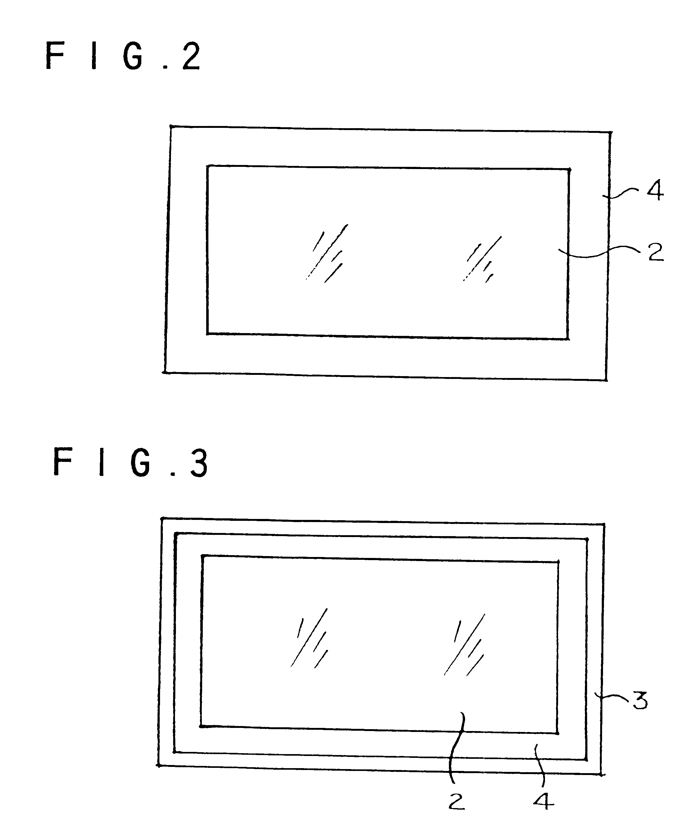
The example will be described with reference to FIG. 1. A glass plate (substrate 1) was cut to have a necessary size followed by chamfering, washing, screen-printing with ink for the colored ceramic layer 4 on the entire periphery of the glass plate as shown in FIG. 3, and drying sufficiently. Then, a silver paste for the electrode 3 was screen-printed on the entire periphery of the glass plate as shown in FIG. 3, and the silver paste was dried. Then, the glass was heated to 660.degree. C., and then, cooled air strengthening was conducted for the purposes of the baking of the ink and the paste and the strengthening of the glass.

On the surface of the thus prepared glass plate on which the electrode 3 was formed, a transparent conductive film (the conductive film 2) was formed by the method described below (the first step).

Namely, the above-mentioned glass plate was set in a sputtering apparatus, and air is discharged to an order of 10.sup.-6 Torr. Then, a multi-conductive fi...

example 2

Two glass plates were cut to be a necessary size, and chamfering operations were conducted to the edge surfaces. To one (substrate 7) of them, a cutout was formed to obtain a position where a terminal for grounding the electrode was formed. To the other glass plate (substrate 1), washing, screen-printing of ink for the colored ceramic layer on the entire periphery of the glass plate as shown in FIG. 3 and sufficiently drying were conducted in the same manner as in Example 1. Thereafter, a silver paste for the electrode was screen-printed on the entire periphery of the glass plate as shown in FIG. 3, and the glass plate was dried.

Then, the glass was heated to 600.degree. C. to bake the ink and the paste. Then, it was annealed to the room temperature. The same transparent conductive film (conductive film) as Example 1 was formed by sputtering on the surface of the glass plate thus formed on which the electrode was formed. Then, the glass plate (substrate 1) was overlaid onto the origi...

example 3

Two glass plates were cut off to be a necessary size, and chamfering operations were conducted to the edge surfaces. To one (substrate 1) of them, washing, was conducted and screen-printing of ink for the colored ceramic layer was conducted on the entire periphery of the glass plate as shown in FIG. 3, and drying sufficiently in the same manner as Example 1. Then, a silver paste for the electrode was screen-printed on the entire periphery of the glass plate as shown in FIG. 3, followed by drying. To the other glass plate (substrate 7), the silver paste for the electrode was screen-printed on the entire periphery of the glass plate and the glass plate was dried in the same manner as substrate 1. No colored ceramic layer was formed.

Both the glass plates (substrate 1 and substrate 7) were heated to a glass temperature of 600.degree. C. to bake the ink and the paste, and they were annealed to the room temperature. The same transparent conductive film (conductive film) as that of Example...


PUM

PropertyMeasurementUnit
temperatureaaaaaaaaaa
thicknessaaaaaaaaaa
thicknessaaaaaaaaaa

Abstract

A protective plate for a plasma display includes conductive substrate for protecting a plasma display and an electrode in electrical contact with the conductive substrate.

Description

1. Field of the InventionThe present invention relates to a protective plate provided at a front face of a plasma display (hereinbelow, referred to as PDP) to protect the main body of PDP and subjected to a treatment for reducing electromagnetic noises and near infrared rays generated from PDP.2. Description of the BackgroundSince a conventional PDP comprises very precise electric components, if it was used as it is and if a user acted on it to apply a force to its surface, there was a high possibility of causing damage. Accordingly, it was necessary to provide protection to prevent the damage.Further, since PDP generates electromagnetic waves harmful to human body and near infrared rays which causes erroneous operations of remote controllers for various kinds of electrical equipments, there has raised necessity for providing a protective plate having a shielding property to the electromagnetic waves.It is an object of the present invention to provide a protective plate for PDP prov...

Claims


Application Information

Patent Timeline
Patent Type & Authority Patents(United States)
IPC IPC(8): G02B1/11G02B1/10G02B5/22G02B5/20H01J17/49B32B7/02B32B17/04G02B1/111G02B1/16G09F9/00H01J17/16H05K9/00
CPCB32B17/10B32B17/10174B32B27/06C03C17/36C03C17/3639C03C17/3644C03C17/3655C03C17/3671C03C17/3676G02B1/11G02B1/116G02B5/208G02B5/22H01J5/02H01J5/03H01J9/241H01J11/10H01J11/44H05K9/0096B32B17/10018Y10T428/315C03C2218/154G09G3/2003G09G2330/06H01J2211/446H01J2211/448B32B17/10005G02B1/14
Inventor SAKURADA, NOBUYOSHIAJIKATA, TOSHIHIROOSADA, KOUICHIMORIWAKI, KENAIKAWA, KATSUAKINODA, KAZUYOSHIOYAMA, TAKUJI
Owner ASAHI GLASS CO LTD
Why Eureka
Try Eureka