

Heterojunction bipolar transistor having prevention layer between base and emitter
a bipolar transistor and prevention layer technology, applied in the direction of transistors, semiconductor devices, electrical appliances, etc., can solve the problems of leak current flow, deterioration of the high frequency characteristic of hbt,
- Summary
- Abstract
- Description
- Claims
- Application Information
AI Technical Summary
Problems solved by technology
Method used
Image

Examples
first embodiment
[First Embodiment]
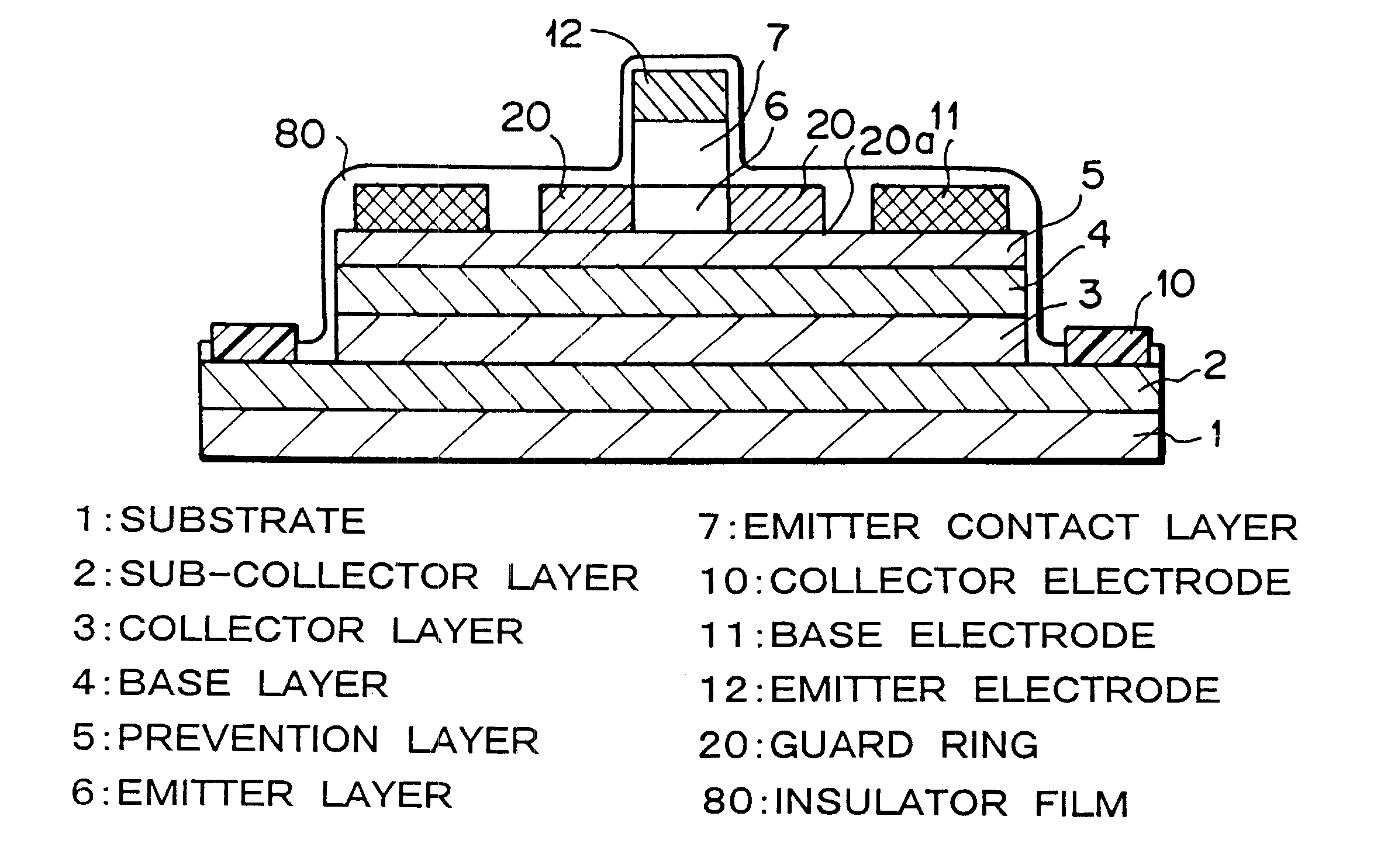
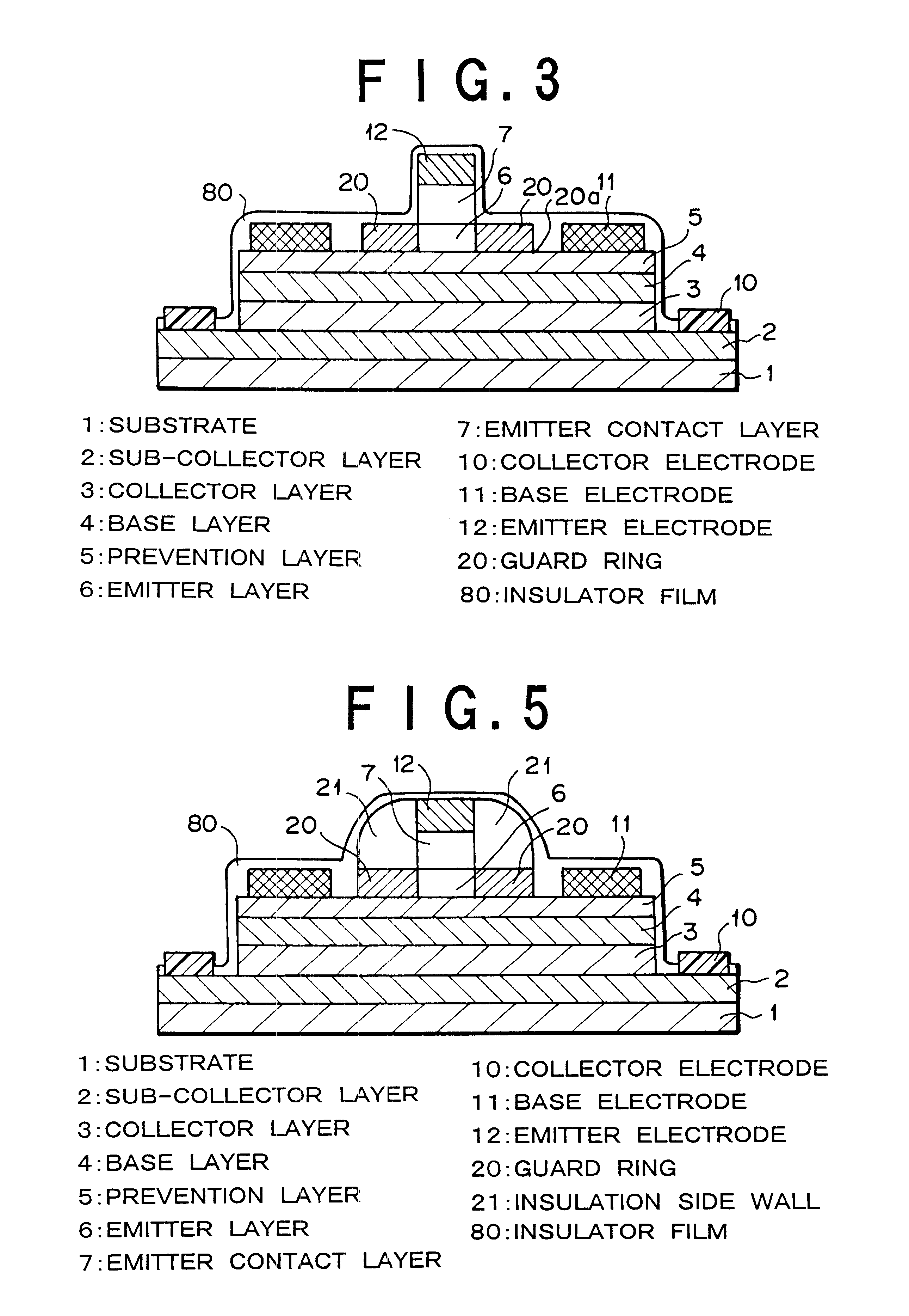
FIG. 3 is a sectional view showing the structure of an HBT according to a first embodiment of the present invention. The HBT shown in FIG. 3 is an InGaP / GaAs NPN type of HBT. A sub-collector layer 2 is grown on a substrate 1. The sub-collector layer 2 is composed of n.sup.+ type of GaAs. The substrate 1 is composed of semi insulating GaAs. A collector layer 3 is grown on the sub-collector layer 2. The collector layer 3 is composed of n type of GaAs.
A base layer 4 is grown on the collector layer 3. The base layer 4 is composed of p.sup.+ type of GaAs. A prevention layer 5 is grown as a thin layer having a thickness of, for example, around 5 nm on the base layer 4 so that carriers are not recombined in the vicinity of the front surface of the base layer 4. The prevention layer 5 is composed of n type of InGaAsP.
The prevention layer 5 and the base layer 4 are grown so that the potential gap of the prevention layer 5 is larger than that of the base layer 4. As a result...
second embodiment
[Second Embodiment]
FIG. 5 is a sectional view showing the structure of an HBT according to a second embodiment of the present invention. The HBT shown in FIG. 5 is different from the HBT shown in FIG. 4 in that an insulation side wall 21 having a thickness of around 100 to 300 nm is formed on a guard-ring 20 using the emitter contact layer 7 as a reference.
The insulation side wall 21 is used as an etching mask when forming the guard-ring 20. After an emitter mesa is formed, an insulation layer is grown on the entire surface of the wafer. Thereafter, the insulation layer is anisotropically etched by a reactive ion etching (RIE) method or the like to form the insulation side wall. The other layer structure and the fabricating steps of the HBT according to the second embodiment are the same as those according to the first embodiment. For simplicity, in FIG. 5, similar portion to those in FIG. 3 are denoted by similar reference numerals.
According to the first embodiment, when the mask i...
third embodiment
[Third Embodiment]
FIG. 6 is a sectional view showing the structure of an HBT according to a third embodiment of the present invention. The structure of the HBT shown in FIG. 6 is the same as the structure of the HBT shown in FIG. 3 except that the former further contains an alloyed region 22 that electrically connects a base electrode 11 and a base layer 4. The alloyed region 22 may contain palladium or platinum.
For example, the alloyed region 22 is formed by heat-treating a base electrode 11 so as to alloy the lowest layer (Pt layer) of the base electrode 11 and a prevention layer 5. Thus, the contact resistance between the base electrode 11 and the base layer 4 becomes small.
PUM
 Abstract
Description
Claims
Application Information