

Stacked structure for memory chips
a technology of memory chips and stacking structures, which is applied in the direction of semiconductor devices, semiconductor/solid-state device details, electrical devices, etc., can solve the problems of large package body volume, difficult signal transmission, and inability to make the package light, thin, short,
- Summary
- Abstract
- Description
- Claims
- Application Information
AI Technical Summary
Problems solved by technology
Method used
Image

Examples
Embodiment Construction
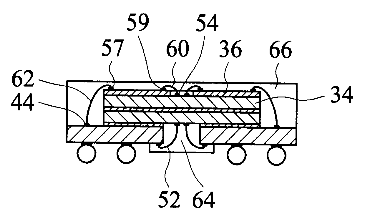
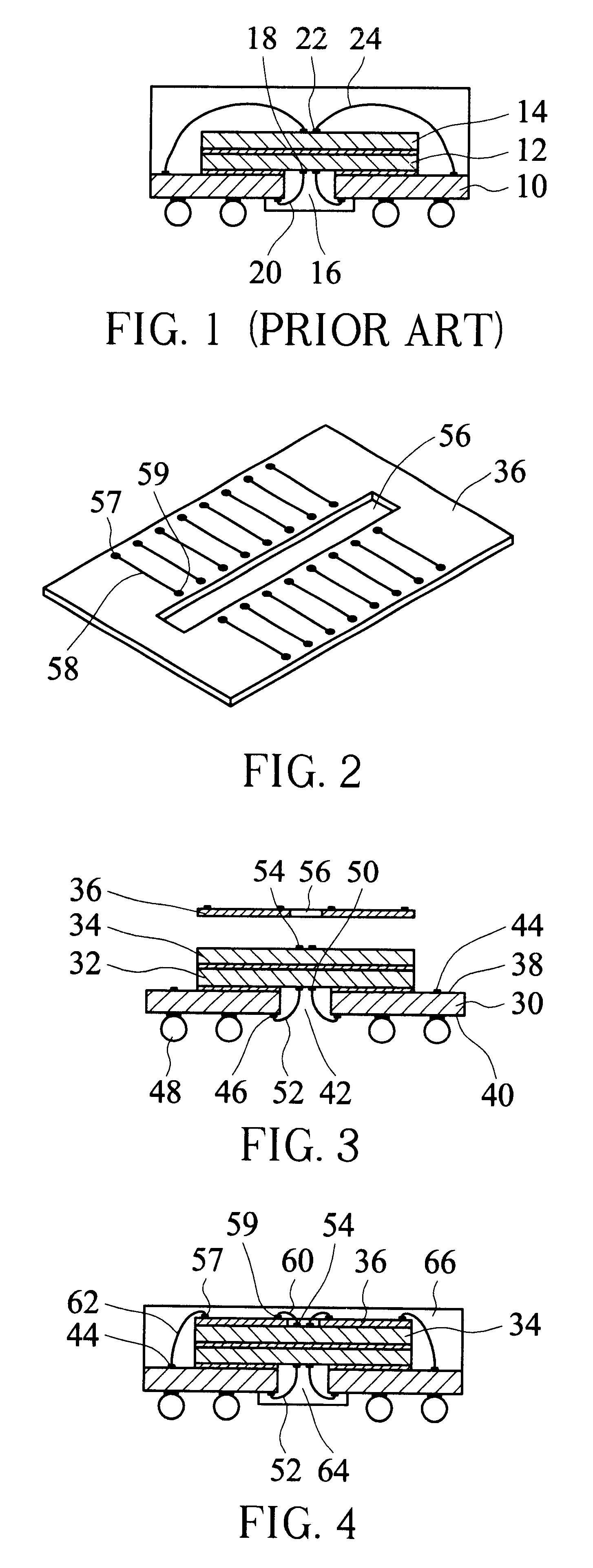
Referring to FIGS. 2 to 4, the stacked structure for memory chips of this embodiment includes a substrate 30, a lower memory chip 32, an upper memory chip 34 and an insulation medium 36.
The substrate 30 has an upper surface 38, a lower surface 40, and a slot 42 penetrating though the substrate 30 from the upper surface 38 to the lower surface 40. The upper surface 38 of the substrate 30 is formed with a plurality of first connection points 44, while the lower surface 40 is formed with second connection points 46 and a plurality of BGA metallic balls 48 at the periphery of the slot 42.
The lower memory chip 32 has a central portion formed with a plurality of bonding pads 50 and is arranged on the upper surface 38 of the substrate 30. The bonding pads 50 are exposed via the slot 42 of the substrate 30. A plurality of wires 52 penetrating through the slot 42 is provided for electrically connecting the bonding pads 50 to the second connection points 46 of the substrate 30, respectively.
T...
PUM
 Abstract
Description
Claims
Application Information