
Method for formation and production of matrices of high density light emitting diodes

a light-emitting diode and high-density technology, applied in the direction of basic electric elements, electrical equipment, semiconductor devices, etc., can solve the problems of poor luminosity, directional dependence of visual impression, slow response speed,

Inactive Publication Date: 2002-11-05
OSRAM GMBH
View PDF6 Cites 15 Cited by
  • Summary
  • Abstract
  • Description
  • Claims
  • Application Information

AI Technical Summary

Problems solved by technology

The use of LCDs include a number of known disadvantages, including poor luminosity, directional dependence for visual impression, and slow response speed.
Even though these problems are not unsolvable, they can for the most part only be coped with by the use of considerable energy.
An additional source of the present problems stems from the characteristics of the active mediums predominant use of liquid crystals.
Such display devices were limited in the past to either display devices of medium informational content such as digital displays, or alphanumerical displays with a low number of pixels in the matrix.
But large area display devices with high informational content have proven to be difficult in the past because of their complexity and high loss capacity.
As a result, large area displays have not emerged from the experimental stage.
Large scale production of large numbers of microscopically small and individually controlled semiconductor light emitting diodes in a tight matrix, i.e. with a very high density, have also not been particularly successful nor satisfactory.
But with this method the LEDs themselves are not individually produced.

Method used


Image

  • Method for formation and production of matrices of high density light emitting diodes
  • Method for formation and production of matrices of high density light emitting diodes
  • Method for formation and production of matrices of high density light emitting diodes

Examples


Embodiment Construction

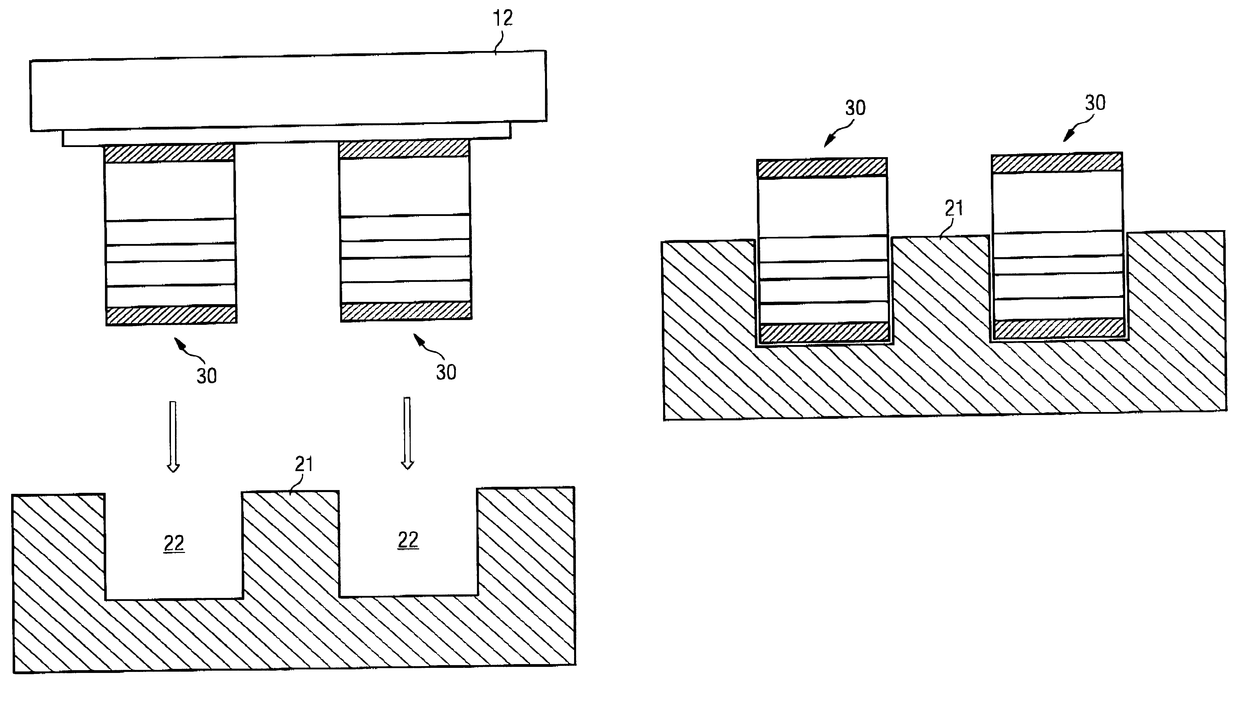
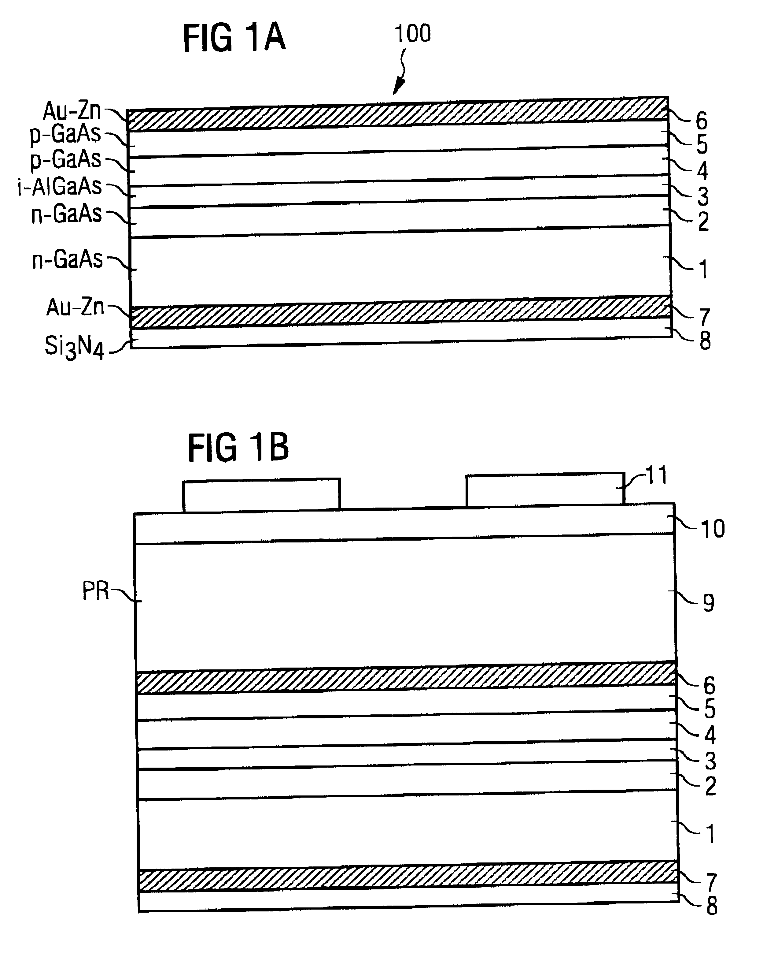
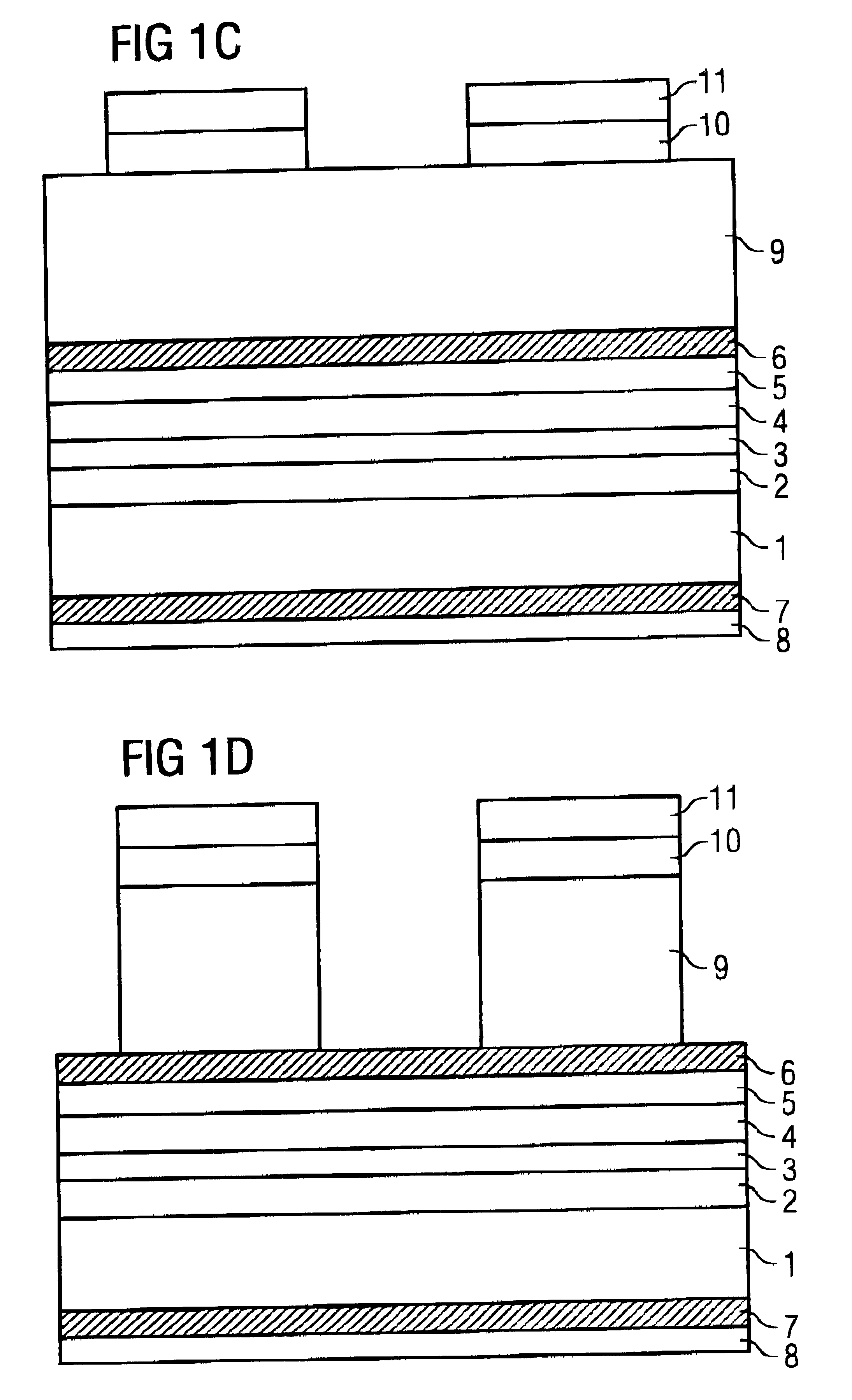
Reference is now made to the figures of the drawings wherein identical or functionally equivalent elements are identified by the same reference numerals. The method according to the invention comprises essentially therein steps for producing periodic deepening pattern by photolithography and reactive etching techniques in a semiconductor device which comprises a LED structure. In further steps, Pillars and pilasters of the semiconductor material are left between the slots, from which the thinned out microscopic semiconductor LEDs are produced. GaAs may be used as a base semiconductor material as set out in more detail below.

First, production of a semiconductor light emission device 100 is set out with initial reference to FIG. 1A. As depicted herein, a n-doped (interference density approx. 10.sup.18 -10.sup.19 cm.sup.-3) GaAs wafer 1 (diameter 2 inches) with a thickness of approx. 100 .mu.m is used as an initial material. A plurality of layers are applied on both sides of the wafer,...


PUM


Abstract

A method for the production and formation of microscopic semiconductor light emitting diodes Is set out. The method comprises the steps of: producing a semiconductor light emitting device (100) including a pn-junction (24) and metallization layers (6, 7); applying an etching mask (9-11) with a preset structure on one side of the semiconductor device (100), whereby the masked areas of the arrangement form and correspond to the diodes to be formed (30); applying a carrier (8, 12) on the other side of the semiconductor device (100); vertically etching the semiconductor material in the openings of the etching mask (9-11) to the carrier (8, 12) and thereby producing a diode arrangement containing a multiple number of diodes (30) below the masked areas. In addition, the method further comprises: removing the etching mask (9-11); providing an accommodating device (20) containing slots (22) with an arrangement and form that correspond to the numerous diodes, whereby the slots are suited for the reception of the diodes (30) therein; engaging the diode arrangement into the accommodating device (20); and removing of the carrier (8, 12). This method can be used for the production of a LED display device having a high pixel density.

Description

1. Field of the InventionThe present invention relates to a method for producing and forming semiconductor light emitting diodes (LEDs), as well as to the production of light emitting display devices formed by the light emitting diodes. In particular, the present invention relates to a method of forming densely packed matrices of semiconductor LEDs which may be individually controlled.2. Description of Related ArtIn the field of display devices and displays in general, conventional cathode radiation tubes are being increasingly replaced, in many areas of application, by flat displays such as liquid crystal displays (LCDs). The use of LCDs include a number of known disadvantages, including poor luminosity, directional dependence for visual impression, and slow response speed. Even though these problems are not unsolvable, they can for the most part only be coped with by the use of considerable energy. This is partly based on the fact that the emitted light displayed by the device in ...

Claims


Application Information

Patent Timeline
Patent Type & Authority Patents(United States)
IPC IPC(8): H01L21/70H01L27/15H01L21/78H01L25/075H01L33/00
CPCH01L21/78H01L25/0753H01L27/156H01L33/0062H01L2924/0002H01L2924/00
Inventor FRANZ, GERHARD
Owner OSRAM GMBH
Learn More