Optoelectronic transceiver module

a technology of optoelectronic transceiver and module, which is applied in the field of optoelectronic transceiver module, can solve the problems of complex method, trivial details, and limited life of silicon mold used in the molding process, and achieves the effects of simple method and simple loading process

Inactive Publication Date: 2003-01-07
HON HAI PRECISION IND CO LTD
View PDF2 Cites 19 Cited by
  • Summary
  • Abstract
  • Description
  • Claims
  • Application Information

AI Technical Summary

Benefits of technology

It is another object of the present invention to provide an optoelectronic transceiver module package that has a robust and tamper resistant design.
Another object of the present invention is to provide a module package design that can easily and quickly be produced.
A further object of the present invention is to provide a module package that can be produced inexpensively.
Therefore, the printed circuit board is retained between and by the frame and the electrical connector. Contrary to the prior art design, the transceiver of the present invention requires no housing to enclose and support the printed circuit board. This simplifies the overall structure. The printed circuit board is surrounded by the metal electromagnetic shielding for protection and elimination of electromagnetic emissions.

Problems solved by technology

For example, it is a time consuming process and it results in a transceiver module which has a pitted outer surface.
In addition, the silicone mold used in the molding process has a limited life of only three to five modules before a new mold must be employed.
Such a method is complicated and loaded down with trivial details.
For example, the structure of the optoelectronic module is complicated and the process is time consuming which cause high costs of manufacturing.

Method used


Image

  • Optoelectronic transceiver module
  • Optoelectronic transceiver module
  • Optoelectronic transceiver module

Examples


Embodiment Construction

Reference will now be made to the drawings to describe the present invention in detail.

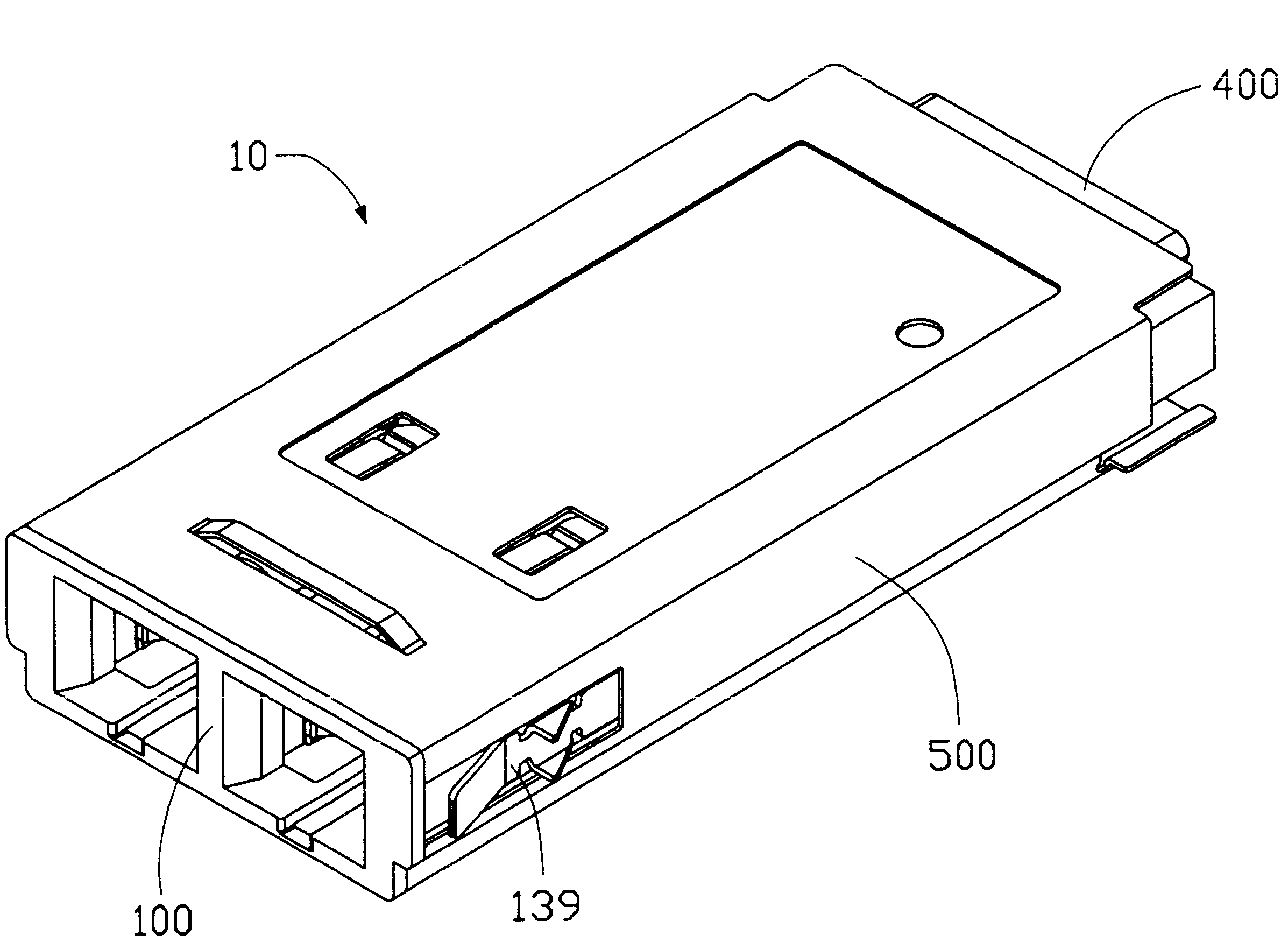
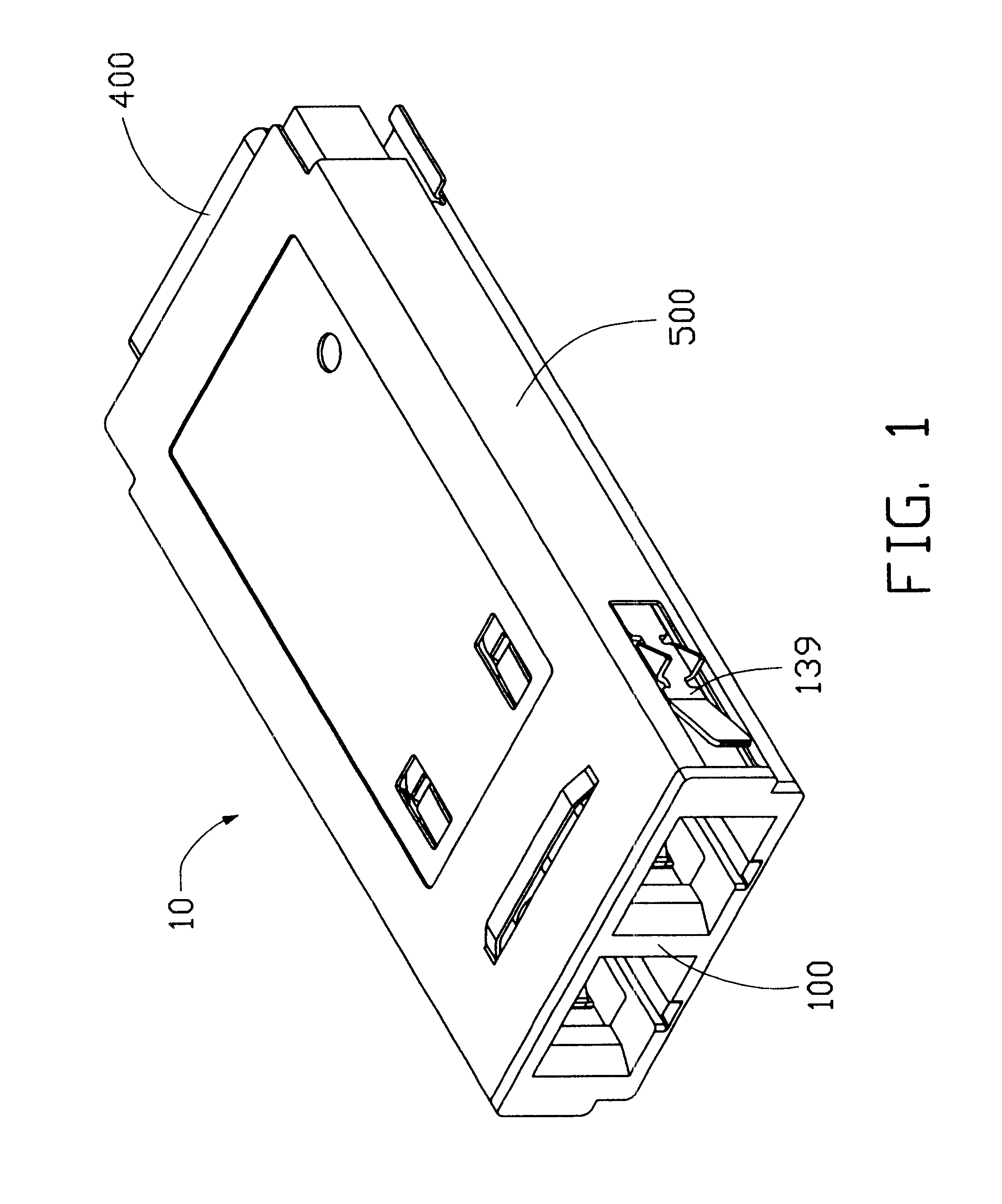
Referring to the drawings, and particularly to FIG. 1, an optoelectronic transceiver module 10 in accordance with the present invention is depicted. The module 10 comprises an assembly 600 as shown in FIG. 2 and an electromagnetic shielding 500 as shown in FIGS. 6A and 6B. Moreover, elementary components of the optoelectronic transceiver module 10 are shown in FIG.7.

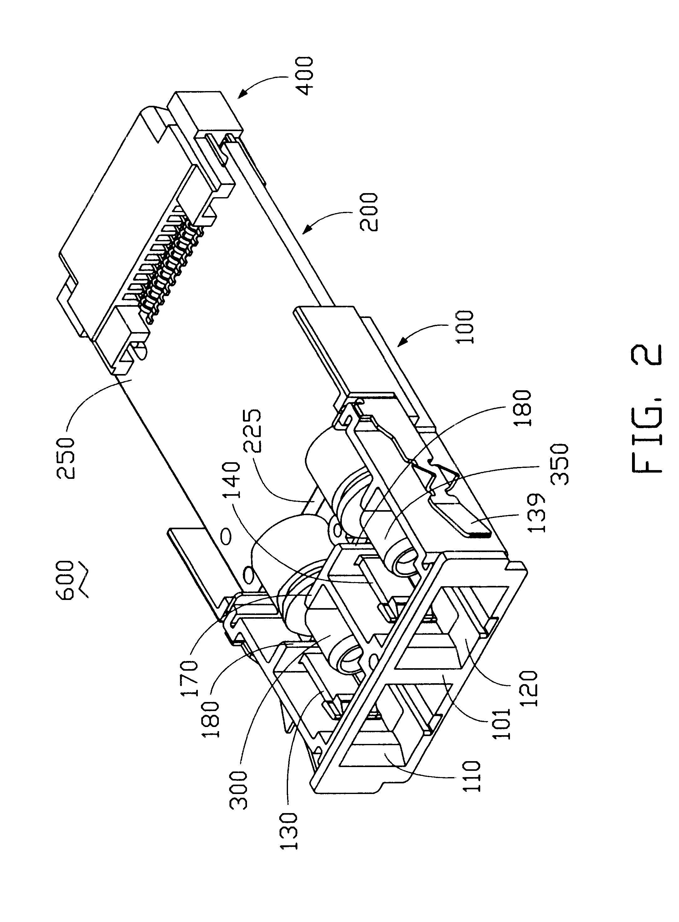
Turning to FIG. 2, the assembly 600 comprises a frame 100 with optical subassemblies 300, 350 mounted therein, a printed circuit board 200 and an electrical connector 400. The optical subassemblies 300, 350 mechanically and electrically connects to a first end 225 of the printed circuit board 200. The electrical connector 400 is mounted to a second end 250 of the printed circuit board 200. Thus, the printed circuit board 200 is fixed between the frame 100 and the electrical connector 400.

Turning to FIG. 3, the frame 100 forms receptacl...


PUM


Abstract

An optoelectronic transceiver module includes an assembly which includes a printed circuit board retained by and between a frame and an electrical connector. An electromagnetic shielding encloses the printed circuit board. The frame forms a receptacle for receiving an optic plug that is optically coupled to an optical subassembly mechanically and electrically connected to the circuit board.

Description

1. Field of the InventionThe present invention relates generally to an optoelectronic transceiver module, and particularly to an optoelectronic transceiver module having a simple structure for enhancing mass production and reducing costs. The present invention also relates to a method for manufacturing the optoelectronic transceiver module.2. Description of Related ArtAn optoelectronic transceiver module provides bi-directional transmission of data between an electrical interface and an optical data link. The module receives electrically encoded data signals which are converted into optical signals and transmitted over the optical data link. Likewise, the module receives optically encoded data signals which are converted into electrical signals and transmitted onto the electrical interface.Normally, the transceiver is mounted on a circuit board of a host computer, an input / output system, a peripheral device, or a switch. Therefore, similar to all electronic equipments, there is a ne...

Claims


Application Information

Patent Timeline
Patent Type & Authority Patents(United States)
IPC IPC(8): G02B6/42
CPCG02B6/4292G02B6/4277
Inventor YEN, CHIA-SUNGHUANG, NAN TSUNGFU, SHAOMING
Owner HON HAI PRECISION IND CO LTD
Why Eureka
Try Eureka