Process for fabricating an MOS device having highly-localized halo regions

a technology of mos device and halo region, which is applied in the direction of semiconductor devices, electrical devices, transistors, etc., can solve the problems of reducing the drive current of transistors, attempting to solve the problem by simply increasing the lateral dimensions of extension regions, and preventing the device from bursting, etc., to achieve the effect of small feature size, easy fabrication, and precise doping profiles

Inactive Publication Date: 2003-01-21
INT BUSINESS MASCH CORP
View PDF20 Cites 37 Cited by
  • Summary
  • Abstract
  • Description
  • Claims
  • Application Information

AI Technical Summary

Benefits of technology

The inventive process continues with the fabrication of elevated source / drain regions 50, as illustrated in FIG. 4. Preferably, a selective epitaxy process is carried out to form elevated source / drain regions 50 to a thickness large enough to avoid silicide formation and contact resistance problems using conventional fabrication procedures. Elevated source / drain regions 50 can be formed by the epitaxial formation of silicon, or alternatively, silicon germanium (SiGe). Preferably, the selective epitaxy process is carried out at a temperature of no more than about 550.degree. C. By maintaining the temperature of the selective epitaxy process at a relatively low value, extensive diffusion of the dopants within first and second halo regions 38 and 48 and extension regions 40 can be avoided.
To electrically activate the dopants previously introduced in thin-film 22, an annealing process is carried out at a temperature of about 900 C. to about 1100 C. Importantly, the process of the invention avoids the application of annealing processes until relatively late in the overall process sequence used to fabricate transistor devices. As a result of the delayed annealing, the thermal budget determined by the designed dimensions of the device is not prematurely exhausted. As illustrated in FIG. 6, the annealing process diffuses the doped regions 54 and 56 into thin-film 22. The delayed annealing feature of the present invention enables relatively precise doping profiles to be formed and maintained within thin-film 22. Accordingly, devices having exceedingly small feature sizes can be readily fabricated using the inventive process. In a preferred embodiment of the invention, the annealing process is carried out by rapid thermal annealing (RTA).

Problems solved by technology

As the gate length of an MOS transistor is reduced to about 0.1 microns or less, the more heavily doped source / drain regions can swamp the extension regions resulting in premature device failure.
Attempts to solve the problem by simply increasing the lateral dimensions of the extension regions fail because the device will experience a substantial increase in parasitic resistance, which reduces the transistor drive current.
Further, complete activation of dopant atoms in the extension regions requires relatively high-temperature thermal annealing.
The high temperature processing causes dopant atoms in the substrate to diffuse, further increasing the series resistance of the device and degrading the rolloff of threshold voltage at short channel lengths.
However, the need for high-temperature thermal annealing to activate dopants also causes the halo regions to diffuse reducing their effectiveness.
However, the threshold voltage instability increases if the halo doping regions, individually formed in the vicinity of the source and drain regions, merge together as a result of lateral diffusion as the devices are scaled to smaller gate lengths.
This problem can exist even at relatively large gate lengths.
Simple geometric tailoring of the halo region doping profile has proven ineffective in the fabrication of MOS transistors having gate lengths on the order of 0.1 microns.
The problem is particularly acute in the fabrication of N-channel devices that require boron implantation to fabricate the halo regions.
Boron implantation is particularly problematic because boron has a relatively high penetration range (Rp) in silicon.
The lateral range, or straggle, of implanted boron makes the fabrication of precisely-configured boron profiles difficult.

Method used


Image

  • Process for fabricating an MOS device having highly-localized halo regions
  • Process for fabricating an MOS device having highly-localized halo regions
  • Process for fabricating an MOS device having highly-localized halo regions

Examples


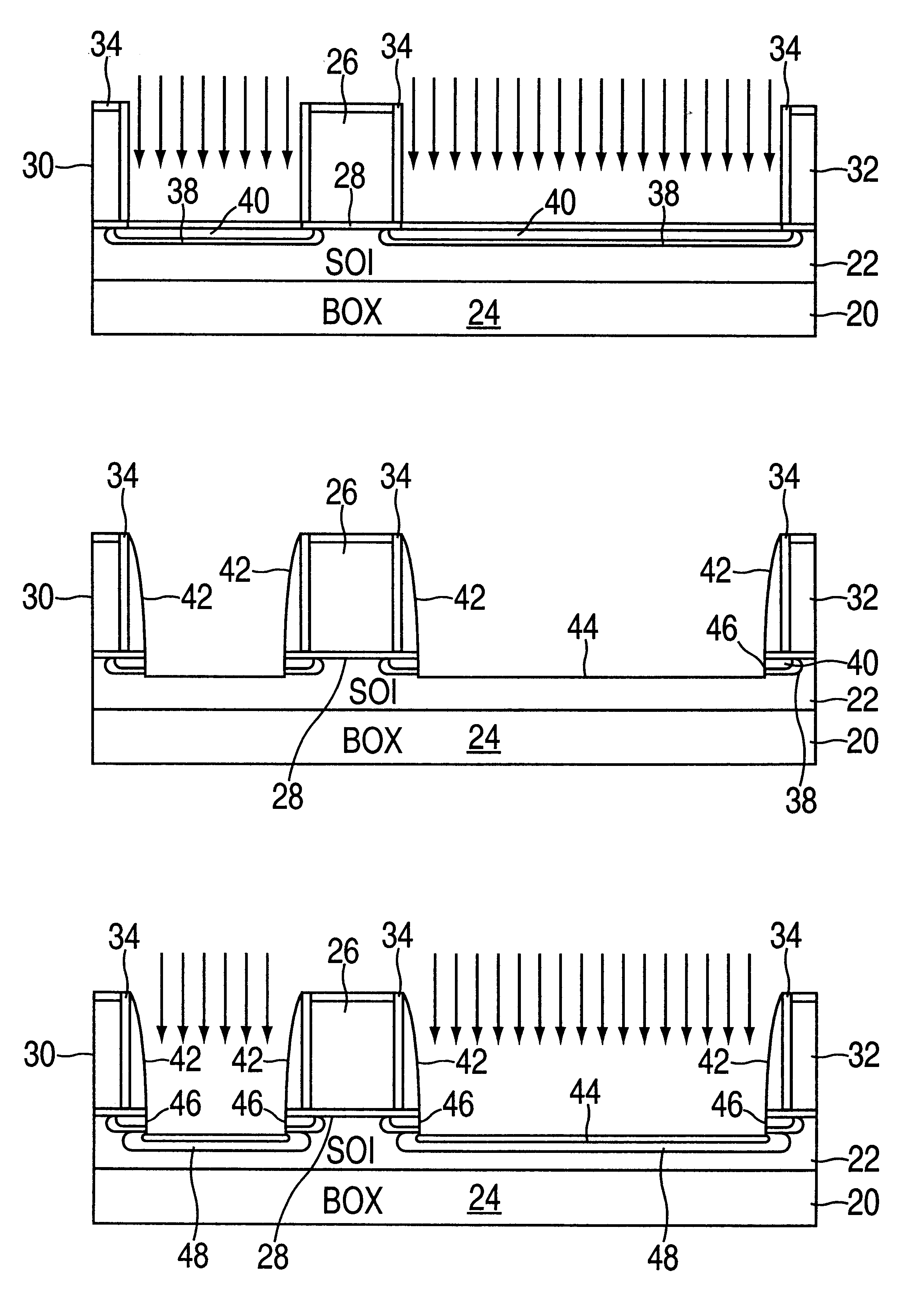
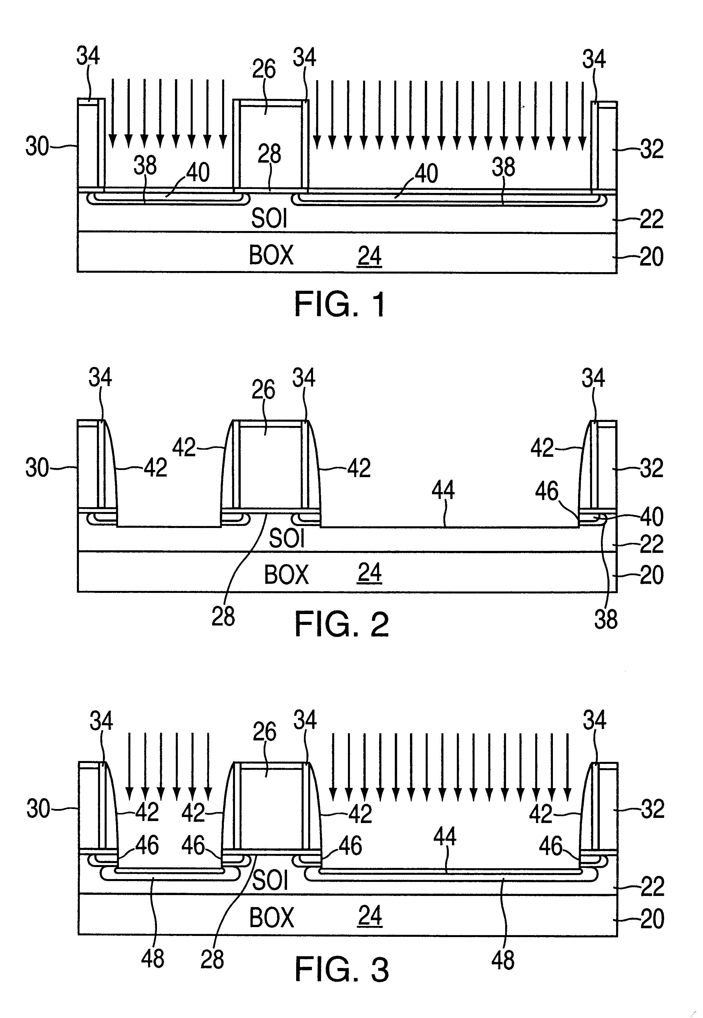
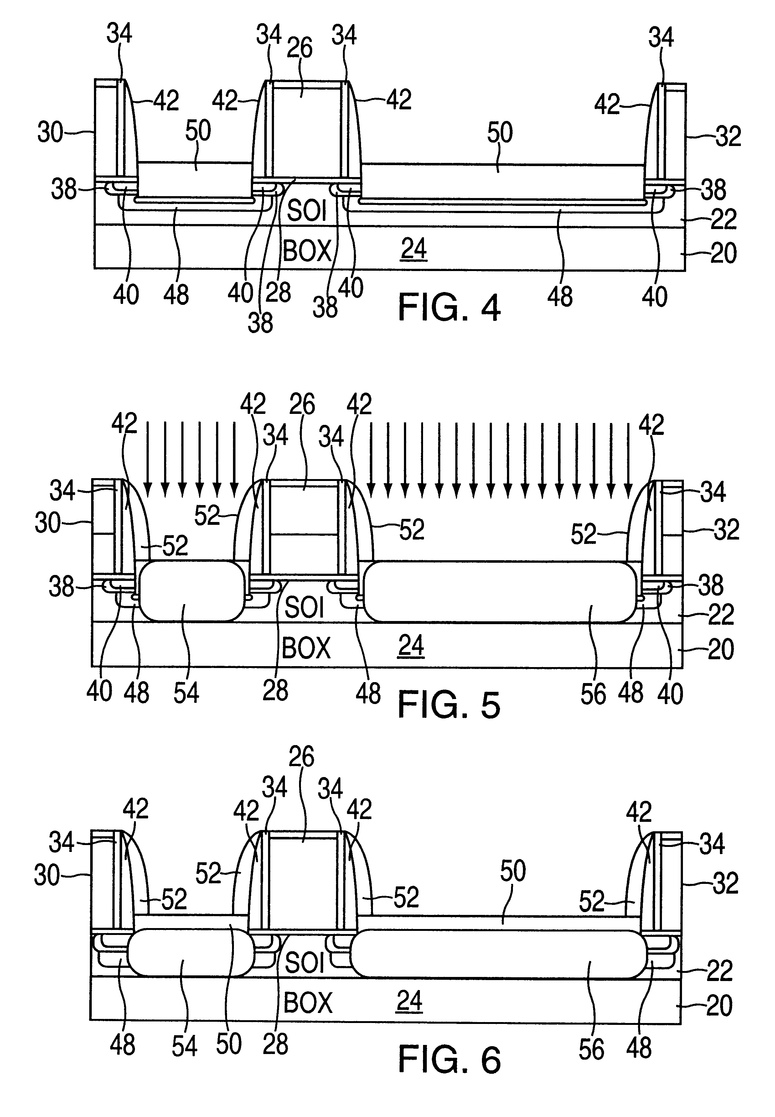
Embodiment Construction

series of Monte Carlo simulation studies were carried out to illustrate the lateral spread of boron implanted into a silicon substrate. FIG. 12 illustrates the results of the Monte Carlo simulation for ion implantation of boron at a dose of 5.times.10.sup.13 cm.sup.-2 at 10 keV into a silicon substrate. The Monte Carlo simulations were carried out using a process simulator UT-MARLOWE (Rel. April, 1999). The simulation shows that the lateral gradient of boron is more than 250 angstroms per decade. After the application of activation annealing, the gradient of the boron halo profile increases more due to transient enhanced diffusion. The lateral spread of the boron halo profile shown in FIG. 12 contributes to short channel effects, such as threshold voltage rolloff, as the gate length is reduced.

The results of a second Monte Carlo simulation are shown in FIG. 13. FIG. 13 shows the results for a boron implantation in the silicon at an energy of 1 keV in a dose of 5E13 ions / cm.sup.2. As...


PUM

PropertyMeasurementUnit
energyaaaaaaaaaa
energyaaaaaaaaaa
gate lengthaaaaaaaaaa

Abstract

A process for fabricating an MOS device having a highly-localized halo region includes the formation of a first halo region at a first surface of a silicon substrate, and a second halo region at a second surface of the silicon substrate. The second surface of the silicon substrate is formed by anisotropically etching the first surface of the silicon substrate to remove a portion of the material from the substrate. Both the first and second halo regions are formed by low-energy ion implantation. For the fabrication of an n-channel device, boron is implanted at an energy of no more than about 1 keV. Upon implantation and a subsequent annealing process, the first and second halo regions form a continuous halo region within the semiconductor substrate.

Description

The present invention relates, generally, to the fabrication of semiconductor devices and, more particularly, to the fabrication of complementary-metal-oxide-semiconductor (CMOS) device structures.Conventional metal-oxide-semiconductor (MOS) transistor fabrication techniques utilize extension regions in the substrate on either side of the channel region below the gate electrode. The extension regions are generally aligned to the gate electrode and are doped at almost the same levels as that of the source / drain regions that are also formed in the substrate on either side of the extension regions. The extension regions function to reduce the electric field gradient in the channel region and minimize hot carrier injection into the gate oxide layer overlying the channel region.As the gate length of an MOS transistor is reduced to about 0.1 microns or less, the more heavily doped source / drain regions can swamp the extension regions resulting in premature device failure. Attempts to solve...

Claims


Application Information

Patent Timeline
Patent Type & Authority Patents(United States)
IPC IPC(8): H01L21/70H01L27/12H01L29/66H01L29/786H01L29/10H01L21/336H01L21/02H01L29/02H01L21/84
CPCH01L21/26506H01L21/26513H01L21/84H01L27/1203H01L29/1045H01L29/1083H01L29/78684H01L29/66628H01L29/66636H01L29/66772H01L29/78621H01L29/665H01L29/165H01L21/2658
Inventor PARK, HEEMYONGMOCUTA, ANDA C.RONSHEIM, PAUL A.
Owner INT BUSINESS MASCH CORP
Why Eureka
Try Eureka