

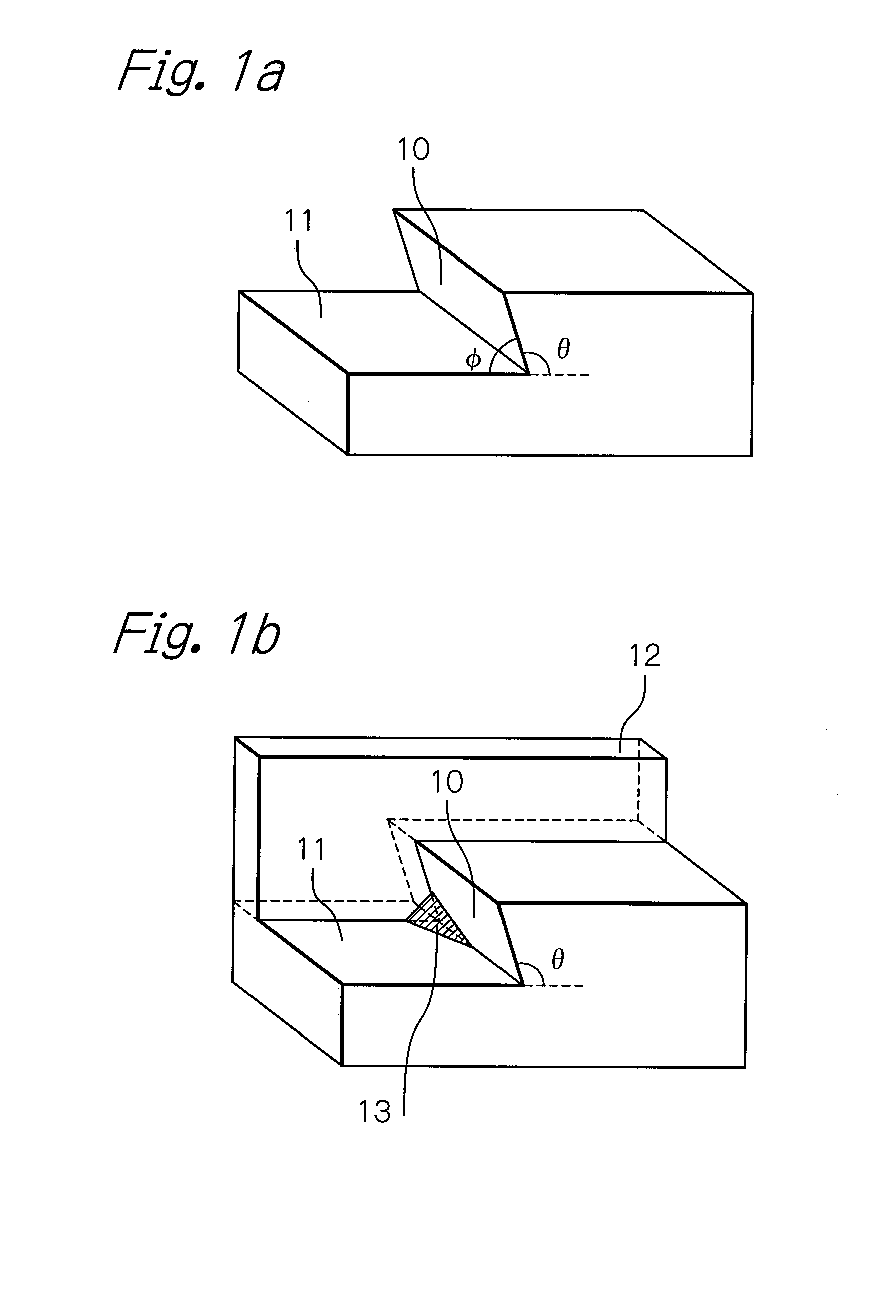
Forming method of resist pattern and manufacturing method of thin-film magnetic head
a technology of resist pattern and manufacturing method, which is applied in the direction of photomechanical treatment originals, instruments, photomechanical equipment, etc., can solve the problems of not applying plating well, not performing sufficient exposure in the shade portion, and not forming desired plating, etc., and achieve the effect of reducing the resolution of the resist pattern
- Summary
- Abstract
- Description
- Claims
- Application Information
AI Technical Summary
Benefits of technology
Problems solved by technology
Method used
Image

Examples
example 1
PRACTICAL EXAMPLE 1
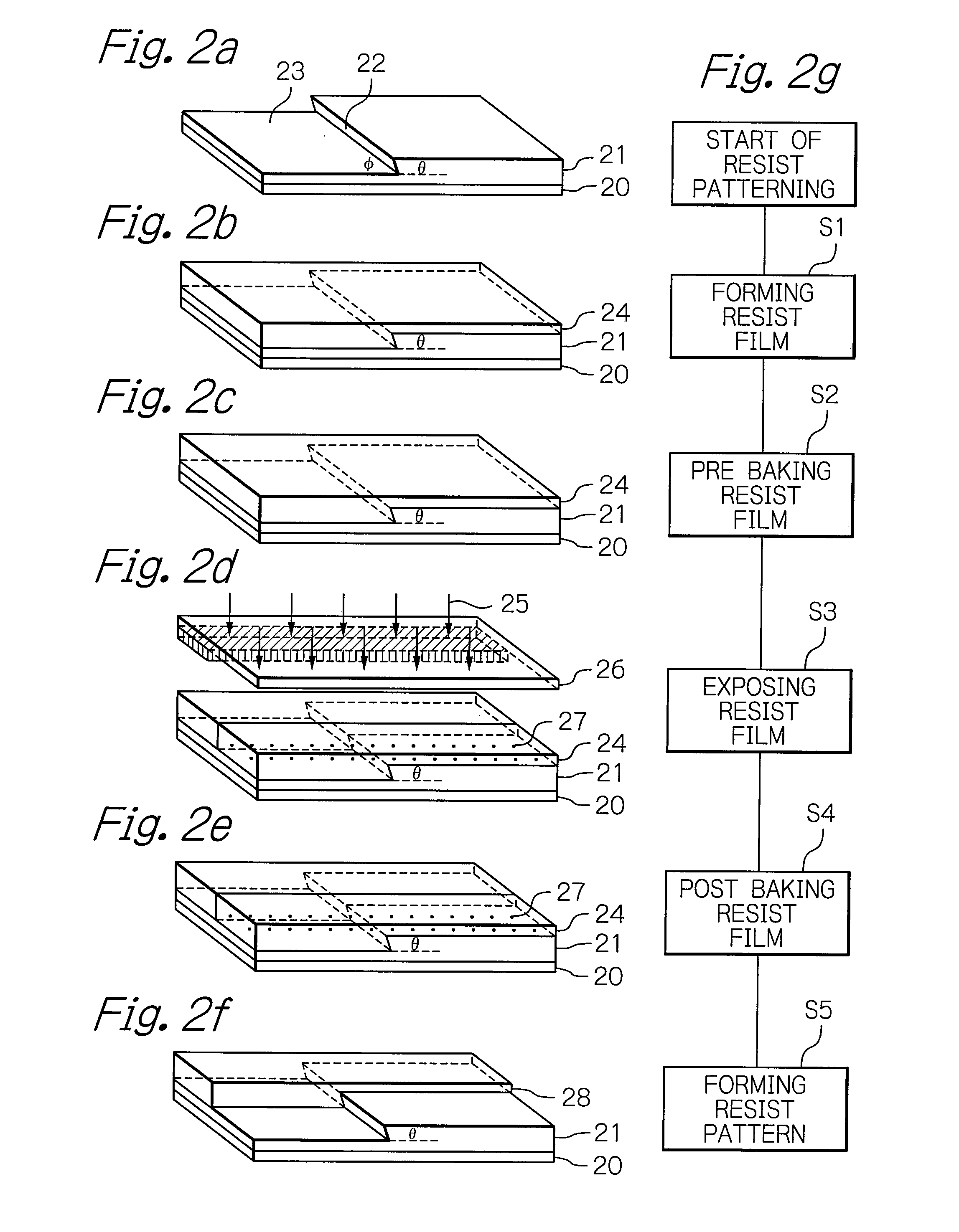
[0054]Table 1 shows an experimental result about a relationship between the pre-bake temperature and the resist residue width WR when the resist pattern is formed on the step formed on the substrate, where the gradient angle of the step is 90 degree or more, using chemically-amplified resist and lowering the temperature of the pre-bake. Also, FIG. 6 is a graph showing an experimental result of Table 1.
TABLE 1Pre bake Temperature (° C.)Resist Residue width (nm)120203100188801436049
[0055]According to the Table 1, it is found that the resist residue width WR reduces with lower and lower the pre-bake temperature. For example, when the pre-bake temperature is 60° C., the resist residue width WR is 49 nm. In this way, the low pre-bake temperature makes the resist residue width WR reduce sufficiently.
[0056]Further, when a plating applies to the resist pattern, the resist residue width WR should be equal to or lower than 100 nm to form a desired plating. Therefore, the pr...
example 2
PRACTICAL EXAMPLE 2
[0062]Table 3 shows an experimental result about the 3σ of the resist width when the resist pattern is formed with chemically-amplified resist, pre-bake at 60° C, and the extend exposure, for comparison, and shows an experimental result about a relationship between the pre-bake temperature and the 3σ of the resist width when the resist pattern is formed with chemically-amplified resist and no extend exposure. FIG. 7 is a graph showing an experimental result of Table 3. Here, the result not to perform the extend exposure is the same as the Table 2. As well as not performing the extend exposure, the experiment obtained the standard deviation σ of the measured values with forming a plurality of the resist patterns whose width is 3.0 μm in the wafer, selecting 40 formed resist patterns, and measuring the resist width of the selected resist patterns.
TABLE 3Pre bake Temperature3σ (40 points in(° C.)wafer) μmExtend Exposure1200.048No800.062No600.075No600.041Yes
[0063]Acco...
PUM
 Abstract
Description
Claims
Application Information