Image scanning circuitry with row and column addressing for use in electronic cameras

a scanning circuit and electronic camera technology, applied in the scanning details of television systems, instruments, television systems, etc., can solve the problems of increasing the scanning speed of the imaging system, requiring high-speed address busses, and adding logic which may be a speed bottleneck

Inactive Publication Date: 2003-01-28
FOVEON
View PDF34 Cites 61 Cited by
  • Summary
  • Abstract
  • Description
  • Claims
  • Application Information

AI Technical Summary

Benefits of technology

Yet another object of the present invention is to provide easy panning control, which changes the start readout location along the vertical and horizontal dimensions of the active pixel sensor array. Each sequential pixel sensor addressing mode allows for an arbitrary pixel sensor readout starting point.
Yet another object of the present invention is to provide a means for selectively complementing the row or column pixel sensor address counting sequence during pixel sensor selection. This feature is useful when the active pixel sensor arrays are used with a color-separation prism whereby some prism outputs may be mirrored. The pixel sensor address complementing feature returns the mirrored prism output to the standard output orientation. The complementing feature is available for both the row and column pixel sensor selection. This allows the active pixel sensor arrays receiving each color separation beam to be placed in any orientation (all vertical or all horizontal, with 180-degree rotation being allowed).
The full frame viewscreen display mode allows the entire high-resolution N rows by M columns pixel sensor array to be displayed onto a viewscreen of lower resolution. The full frame viewscreen mode, by counting in steps of Kn for row addressability and counting in steps of Km for column addressability, selectively skips rows and columns of the active pixel sensor array when selecting pixel sensors to display onto the viewscreen. This selective skipping allows the higher-resolution pixel array to be mapped onto the lower-resolution viewscreen. Selective pixel sensor skipping will cause some image detail to be lost, but the user will be able to see a lower-resolution version of the entire image.
Complementors are also included in each row and column address counter, allowing for image mirroring in both the X and Y directions. The use of a color-separation prism within the camera to resolve the incoming image into three color channels means that one or more of the color separation beams may have an orientation that is mirrored with respect to the other color separation beams. The X and Y complementors allow the orientation of a particular color separation image to be reversed, putting it back into the correct orientation to be recombined with the other color separation beams.

Problems solved by technology

This technique increases the scanning speed of the imaging system while decreasing the resolution of the sensor array data.
However, such systems involve additional circuitry to average the pixel sensor values.
In prior-art systems using random-access imager arrays, external logic could be used to select rows and columns for pan and zoom, but this requires high-speed address busses and added logic which may be a speed bottleneck.
However, this type of color separation prism has the disadvantage of requiring an air gap within the prism itself to achieve the same image orientation for all three-color separation beams.
Such prisms can be difficult to manufacture properly.
It is not possible to display all pixels from the high-resolution pixel array onto the viewscreen, and a method for selecting which pixels to display is necessary.
This full image capture mode of readout is too large to fully display onto the low-resolution viewscreen.
Selective pixel sensor skipping will cause some image detail to be lost, but the user will be able to see a lower-resolution version of the entire image.

Method used


Image

  • Image scanning circuitry with row and column addressing for use in electronic cameras
  • Image scanning circuitry with row and column addressing for use in electronic cameras
  • Image scanning circuitry with row and column addressing for use in electronic cameras

Examples


Embodiment Construction

Those of ordinary skill in the art will realize that the following description of the present invention is illustrative only and not in any way limiting. Other embodiments of the invention will readily suggest themselves to such skilled persons.

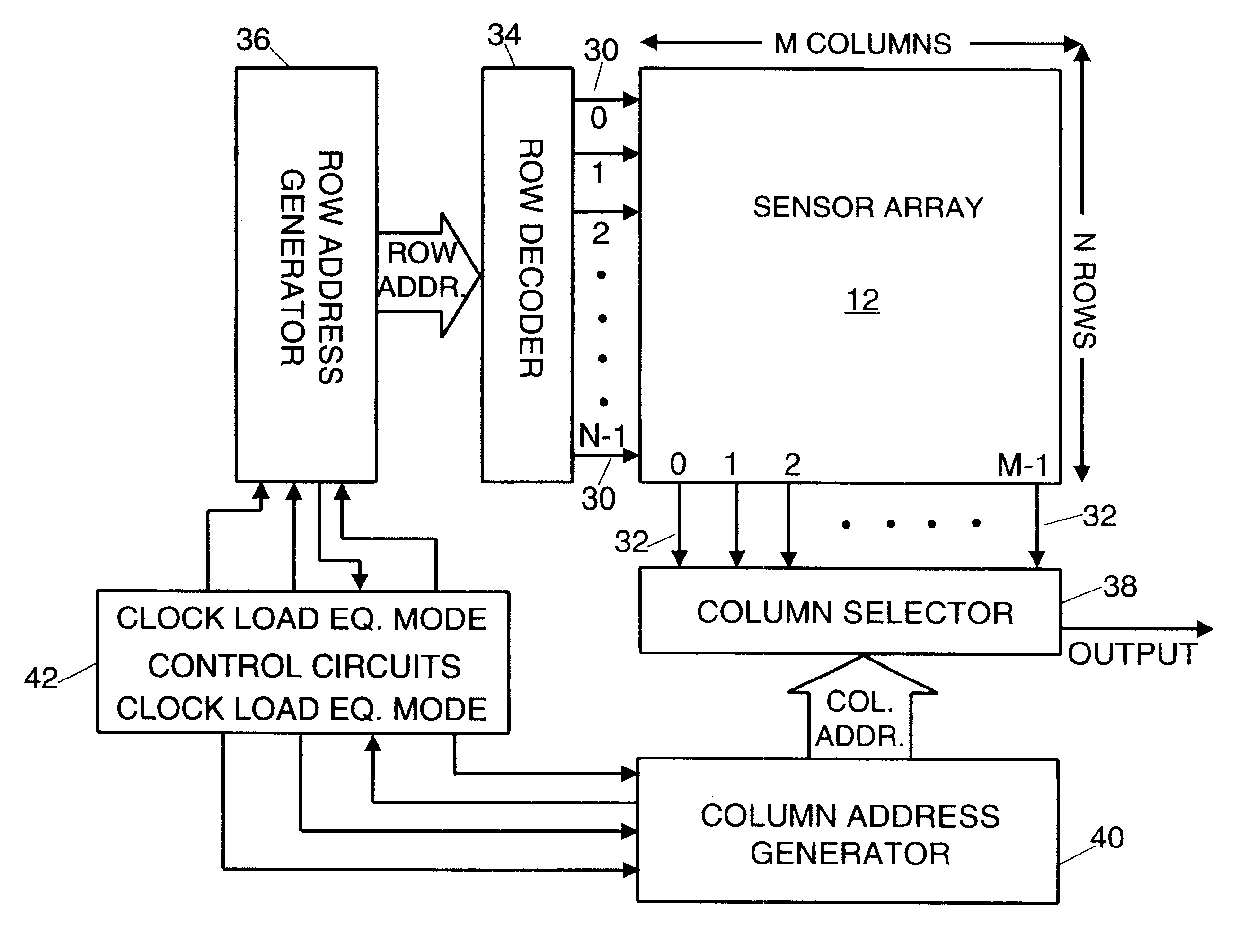
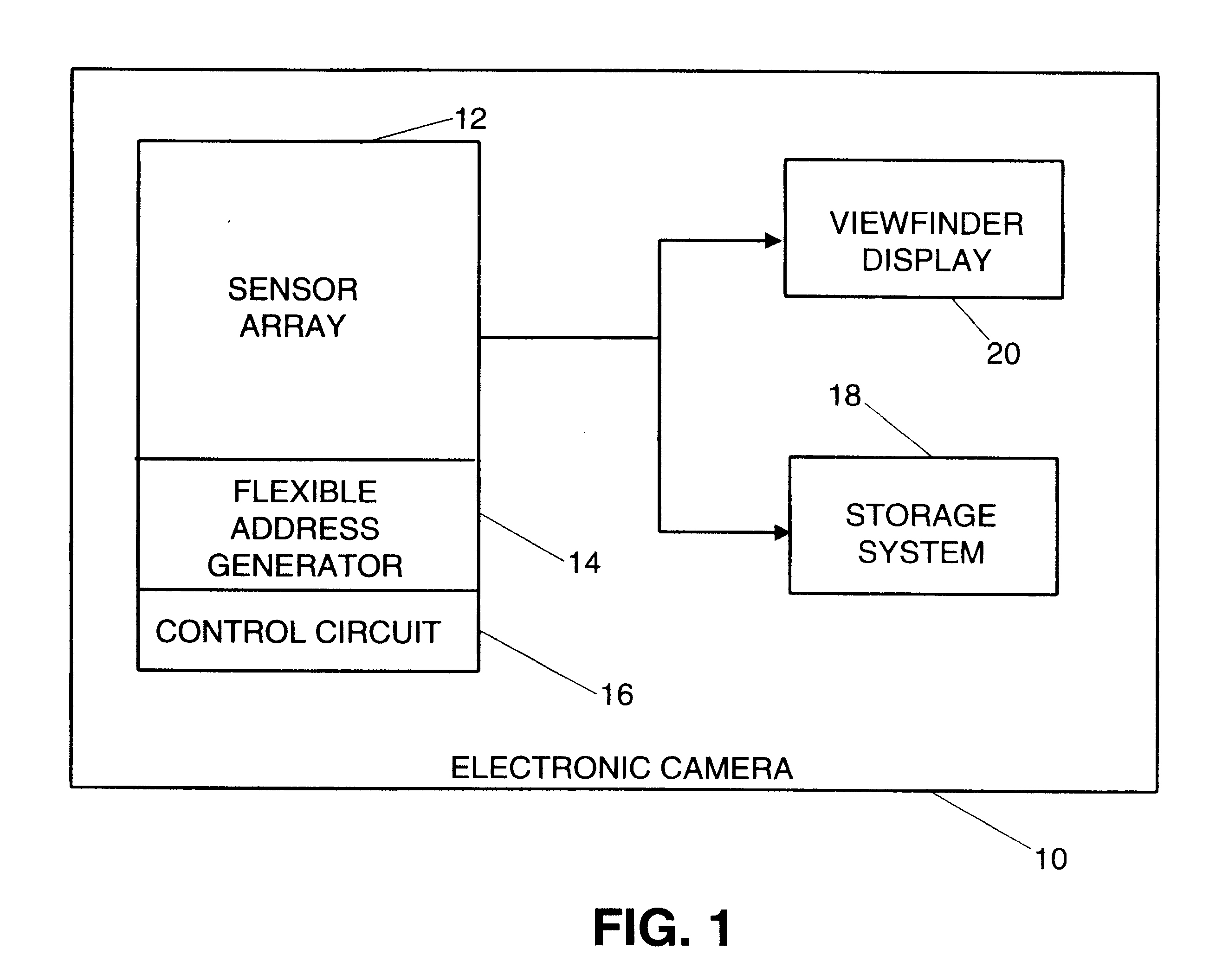
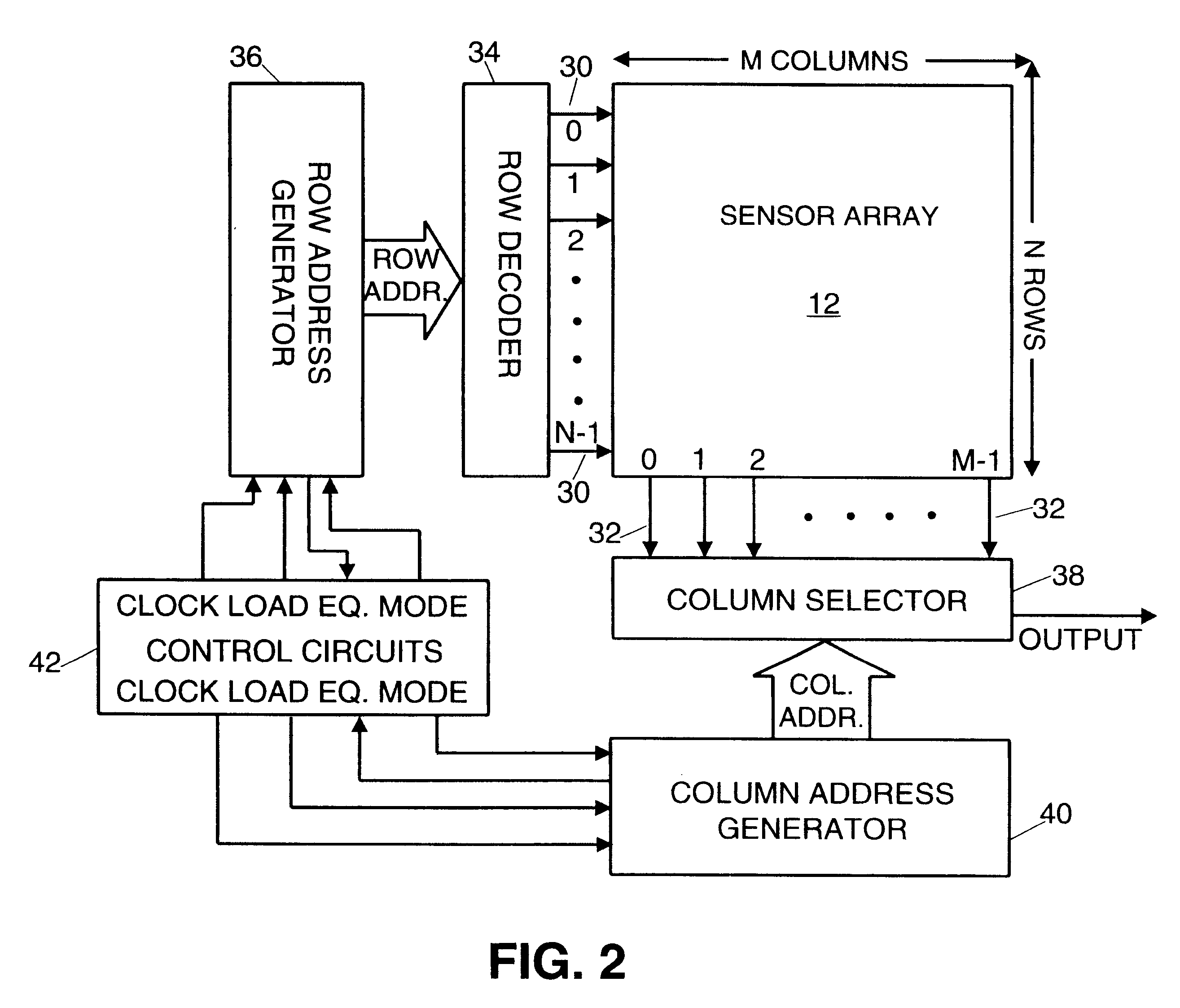
Referring first to FIG. 1, a block diagram of an electronic camera 10 employing the scanning circuitry of the present invention is shown. Electronic camera 10 includes a pixel sensor array 12, such as an active pixel sensor array. According to the present invention, pixel sensor array 12 is controlled by a flexible address generator circuit 14. Flexible address generator circuit 14 is controlled by a control circuit 16 that provides all of the signals necessary to control reading pixel data out of the array 12. The flexible address generator circuit 14 and control circuit 16 may be used to read full high-resolution image data out of the pixel sensor array 12 and store that data in storage system 18. The pixel sensor array 12 is a high-resolut...


PUM


Abstract

A scanning circuit for use with an active pixel sensor array comprises a row-address generator configured to start at a selected row-start address, stop at a selected row-stop address, and increment row addresses by a factor K. A column-address generator is configured to start at a selected column-start address, stop at a selected column stop address, and increment column addresses by a factor K. Circuitry is coupled to the row address generator and the column address generator, for storing the row-start address, the row-stop address, the column-start address, the column-stop address and the factor K. A row decoder is coupled to the row-address generator and a column selector is coupled to the column-address generator. A plurality of row select lines are coupled to the row decoder, each one of the row select lines associated with a different row in the active pixel sensor array. A plurality of column output lines are coupled to the column selector, each one of the column output lines associated with a different column in the active pixel sensor array.

Description

1. Field of the InventionThe present invention relates to image sensor array technology for use in electronic cameras employing solid state pixel sensor arrays. More particularly, the present invention relates to image scanning techniques for displaying a high-resolution image sensor pixel array onto a viewscreen of lower resolution.2. The Prior ArtActive pixel sensor arrays are well known in the prior art. Readout techniques for active pixel sensor arrays combine pixel sensor addressing schemes with scanning circuitry suitable for reading solid state sensor arrays. Exemplary scanning circuitry suitable for vertical and horizontal scanning is described in Analog VLSI and Neural Systems, by Carver A. Mead, Addison Wesley Publishing Co., 1989, at pp. 263-267.Pictures from active pixel sensor arrays are often displayed onto viewscreens which have a lower resolution than the active pixel sensor array itself does. In order to fit the picture onto the viewscreen, some pixels are not displ...

Claims


Application Information

Patent Timeline
Patent Type & Authority Patents(United States)
IPC IPC(8): H04N3/15H04N5/343H04N5/374H04N5/376
CPCH04N3/1562H04N3/155H04N25/443H04N25/745H04N25/76
Inventor LYON, RICHARD F.TURNER, RICHARD M.MERRILL, RICHARD B.
Owner FOVEON
Why Eureka
Try Eureka