Semiconductor device and electric power conversion device

a technology of semiconductor devices and electric power conversion devices, which is applied in the direction of dc-ac conversion without reversal, solid-state devices, electric cable installations, etc., can solve the problems of the occurrence of voltage exceeding the voltage of the element and the loss at the time of switching increases

Inactive Publication Date: 2003-02-25
HITACHI LTD
View PDF11 Cites 57 Cited by
  • Summary
  • Abstract
  • Description
  • Claims
  • Application Information

AI Technical Summary

Problems solved by technology

The above-described prior arts reduce the inductances individually in the semiconductor device inner-wiring and the wiring of connecting the electrolytic capacitor with the semiconductor device in th...

Method used


Image

  • Semiconductor device and electric power conversion device
  • Semiconductor device and electric power conversion device
  • Semiconductor device and electric power conversion device

Examples


Embodiment Construction

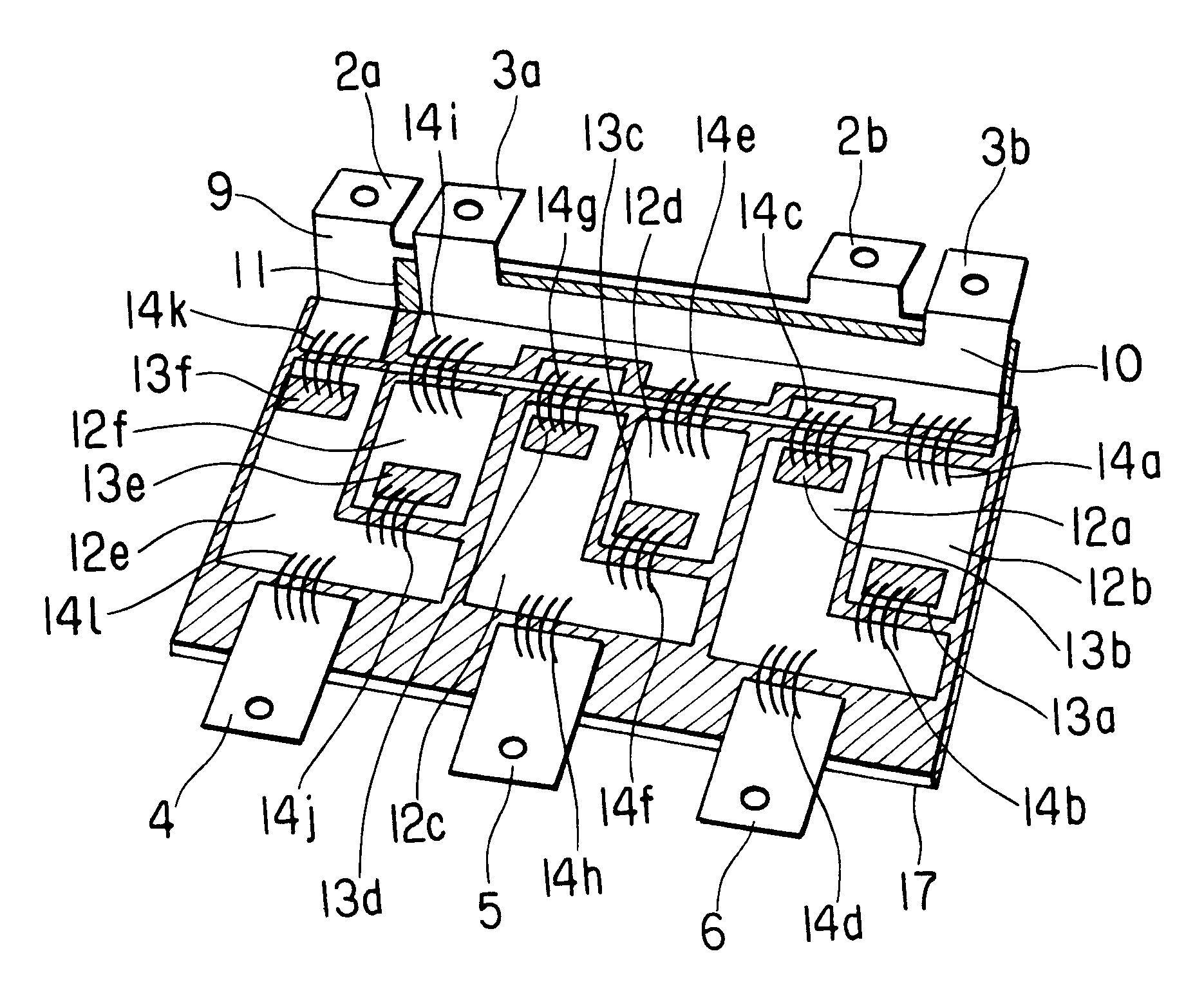
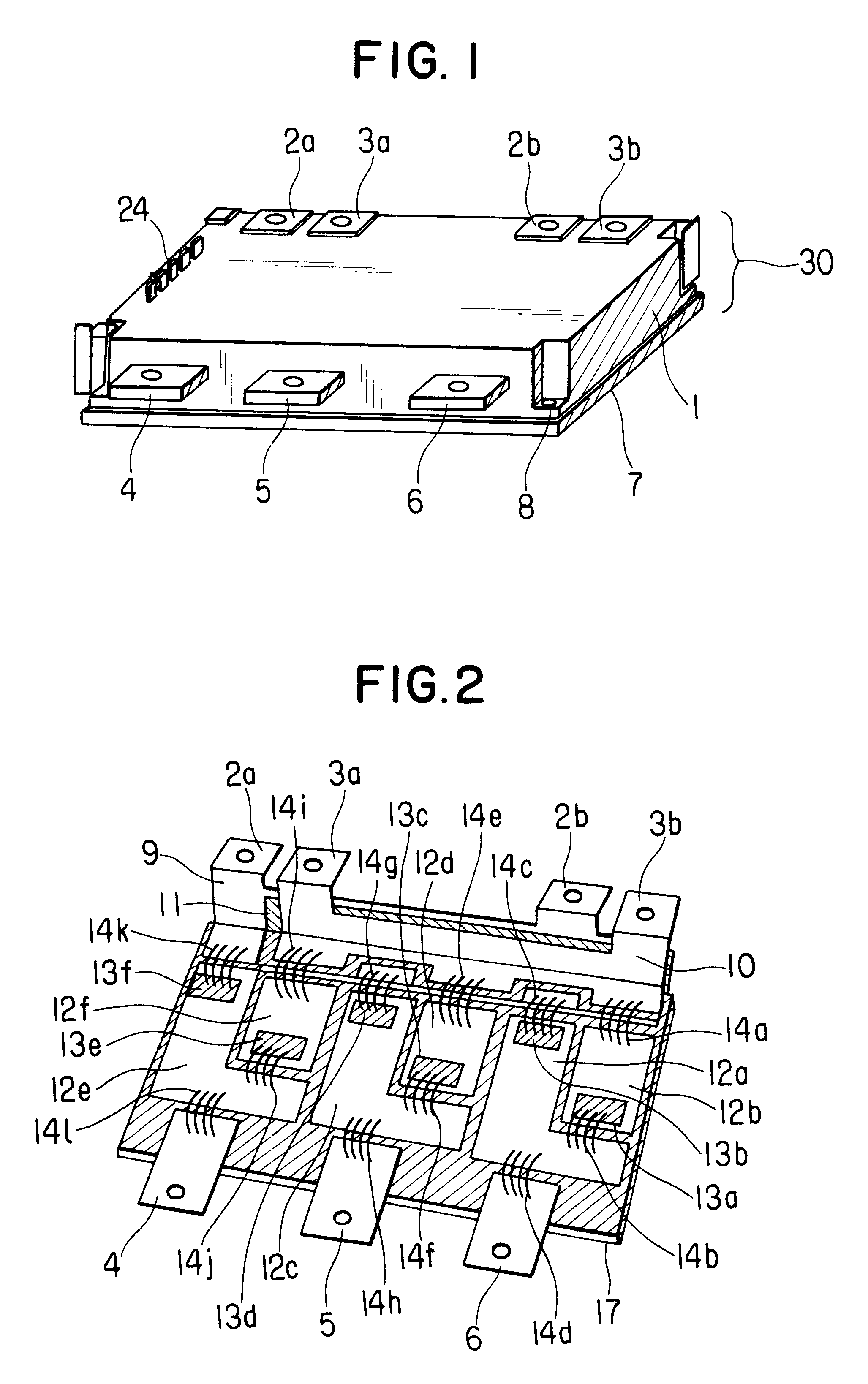
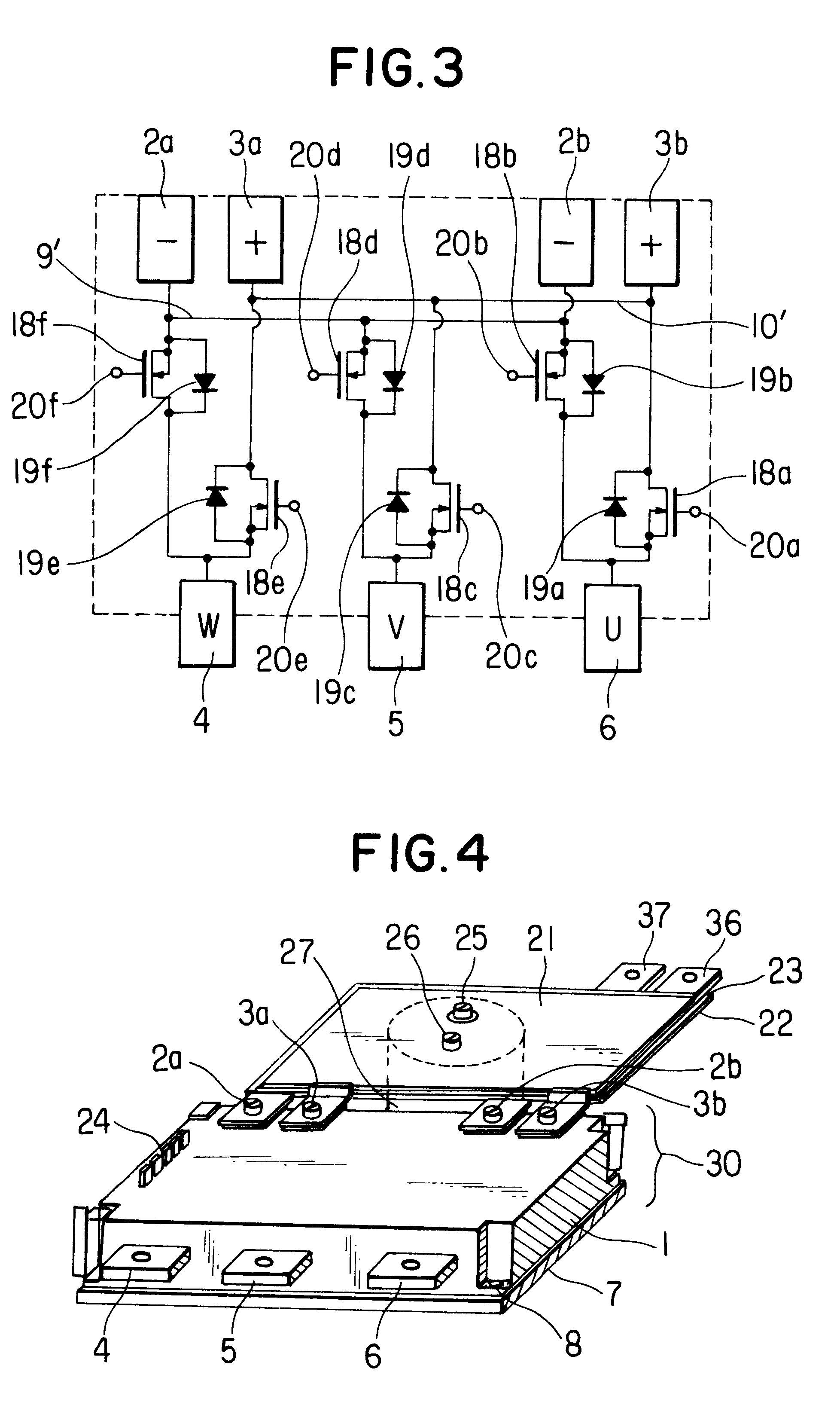
Hereinafter, based on FIGS. 1 to 9, the explanation will be given concerning embodiments of the present invention. In FIGS. 1 to 9, the same reference numeral is assigned to the same configuration component or a configuration component having the same function. Also, in order to make the accompanying drawings easy to understand, a driving circuit for driving semiconductor switches is omitted.

FIG. 8 illustrates an example of the circuit configuration of the electric power conversion device. In FIG. 8, the reference numerals denote the following components, respectively: 30a, 30b semiconductor devices, 31 a 3-phase alternating current power supply, 32 input wires, 33a a main circuit wiring, 33b a main circuit wiring, 27 an electrolytic capacitor, 34 output wires, 35 an induction motor (which is also refereed to as a load). The semi-conductor devices 30a, 30b include power semiconductor switch elements such as an IPM, a power MOSFET (Metal Oxide Semiconductor Field Effect Transistor) a...


PUM


Abstract

A semiconductor power conversion device includes two bridge-connected semiconductor switches, an output terminal, and first and second pairs of positive and negative direct current terminals. First conductors connect the negative direct current terminals of the first and second pairs with the output terminal through one of the two bridge-connected semiconductor switches, while second conductors connect the positive direct current terminals of the first and second pairs with the other of the two bridge-connected semiconductor switches. A housing is provided, which includes the two bridge-connected semiconductor switches, and at least a portion of the first conductor and of the second conductor as a multilayer structure formed by sandwiching an insulator between the first and second conductors inside the housing. The first and second pairs of direct current terminals are arranged on one side of one plane of the housing.

Description

1. Field of the InventionThe present invention relates to a semiconductor device and an electric power conversion device.2. Description of Related ArtConventionally, JP-A-7-311552 has disclosed an inner wiring structure of a semiconductor device, and JP-A-8-140363 has disclosed a wiring structure of connecting an electrolytic capacitor with the semiconductor device in an electric power conversion device. These technologies have disclosed the formation of a multilayer structure with an objective that, in the semiconductor device inner-wiring and the wiring of connecting the electrolytic capacitor with the semiconductor device in the electric power conversion device, the direction of an electric current flowing in a positive-polarity side wiring and that of an electric current flowing in a negative-polarity side wiring becomes opposite to each other. Here, an object of the above-described formation is to decrease inductances that become the causes of an increase in the loss at the tim...

Claims


Application Information

Patent Timeline
IPC IPC(8): H02M7/00H01L25/07H01L25/18H02M1/00H02M7/48
CPCH02M7/003H01L2924/0002H01L2924/00H01L2224/49111H01L2924/19107
Inventor SHIRAKAWA, SHINJIFUKUMOTO, HIDESHIMISHIMA, AKIRAMASHINO, KEIICHIINNAMI, TOSHIYUKI
Owner HITACHI LTD
Why Eureka
Try Eureka