

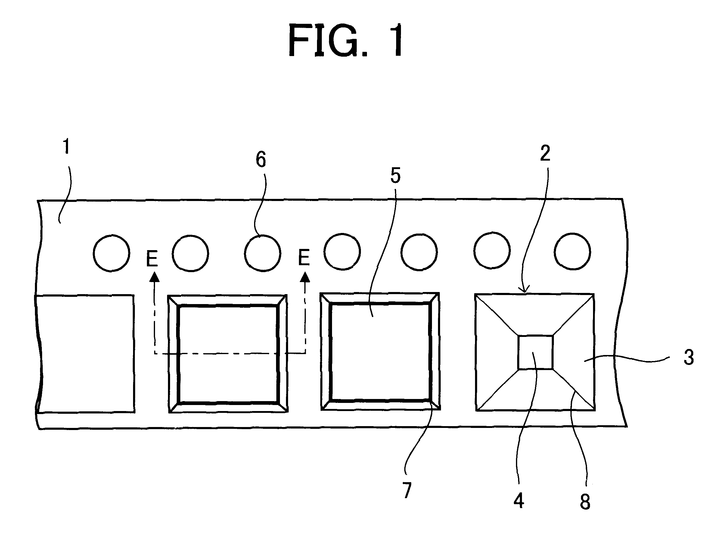
Embossed carrier tape
a carrier tape and tape strip technology, applied in the field of embossed carrier tape, can solve the problems of unstable position of electronic devices, inability to take out electronic devices, and easy movement of electronic devices within the pockets, and achieve the effect of easy adsorption
- Summary
- Abstract
- Description
- Claims
- Application Information
AI Technical Summary
Benefits of technology
Problems solved by technology
Method used
Image

Examples
first preferred embodiment
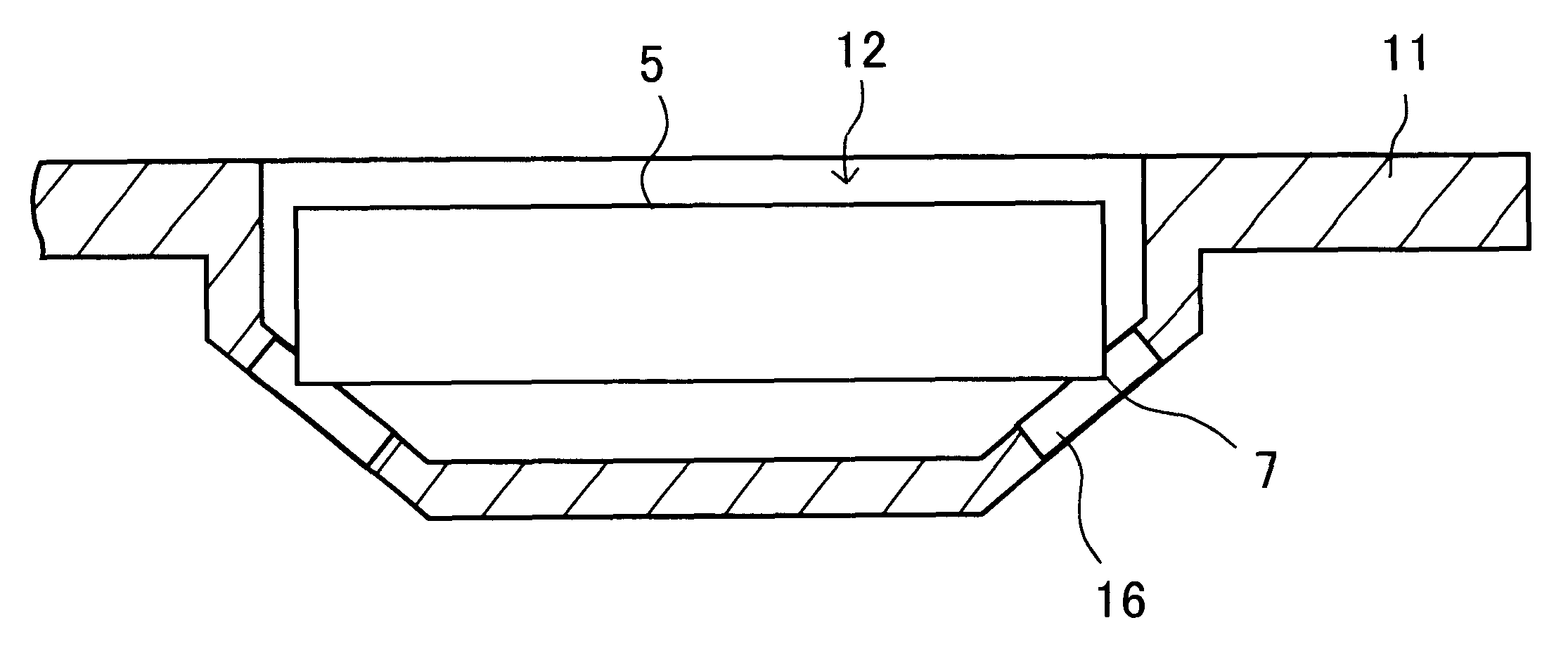
FIG. 3 is a plan view showing a part of an embossed carrier tape according to a first preferred embodiment of the present invention. FIG. 4 is a cross-sectional view taken on line A--A in FIG. 3. An embossed carrier tape 11 according to the first preferred embodiment includes a plurality of pockets (device holes) 12 in which electronic devices 5 are held. Each of the pockets (device holes) 12 is shaped to be a reverse quadrangular pyramid having inner side surfaces 13, a bottom surface 14 and openings 16. The inner side surfaces are separated by ridge lines (inside edge line). The openings 16 are formed along the ridge lines (inside corner lines) 15.
An electronic device 5 is supported around its corners 7 in the concavity 27. The corners 7 of the electronic device 5 are not in contact with the inner side surface 23 or the ridge lines 25. Each of the concavities 27 is formed integrally with the embossed carrier tape 21, so that an electronic device 5 is in contact at the bottom with ...
second preferred embodiment
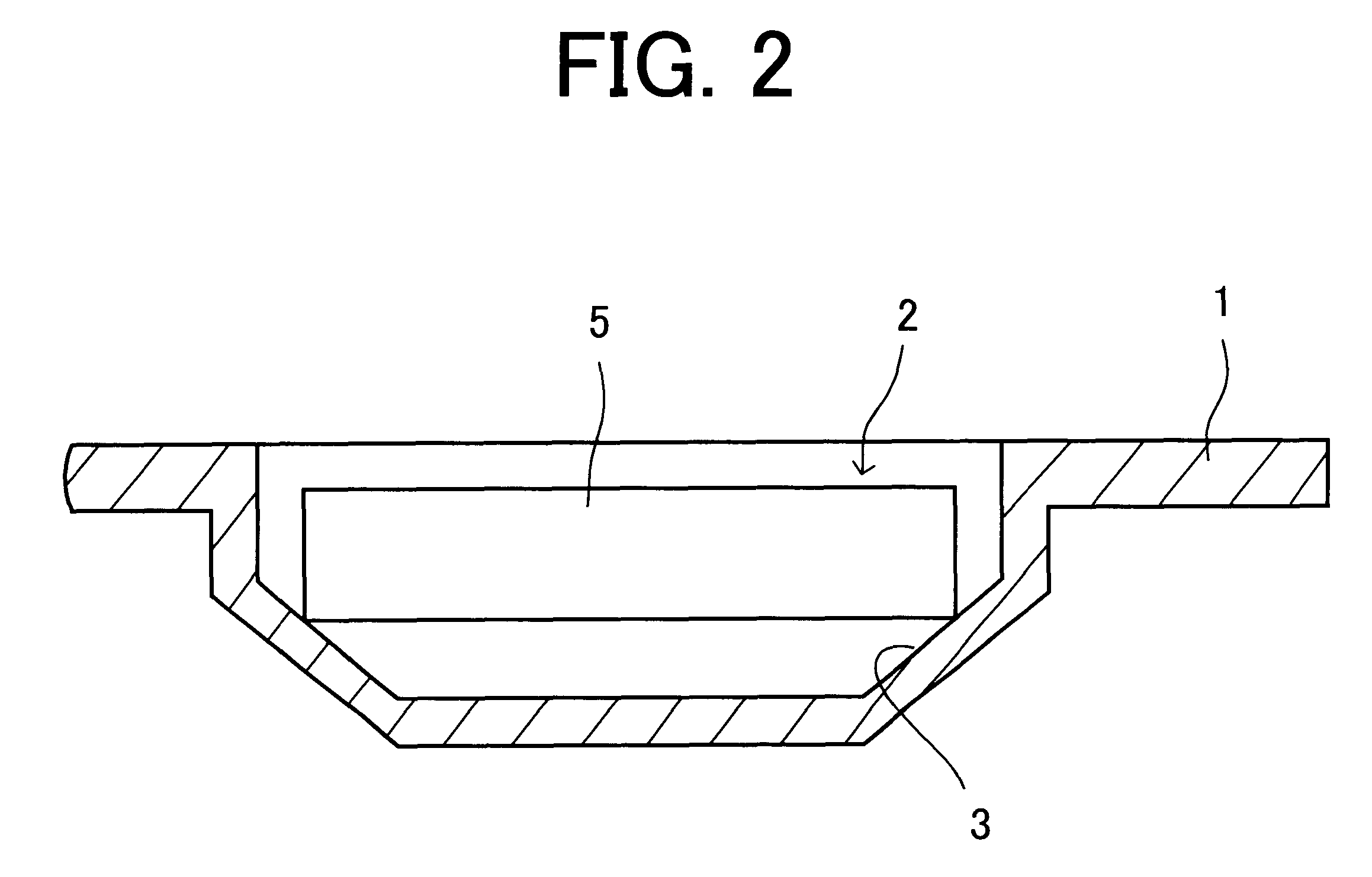
FIG. 5 is a plan view showing a part of an embossed carrier tape according to a second preferred embodiment of the present invention. FIG. 6 is a cross-sectional view taken on line B--B in FIG. 5. An embossed carrier tape 21 according to the second preferred embodiment includes a plurality of pockets (device holes) 22 in which electronic devices 5 are held. Each of the pockets (device holes) 22 is shaped to be a reverse quadrangular pyramid having inner side surfaces 23, a bottom surface 24 and concavities 27. The inner side surfaces are separated by ridge lines (inside edge line). The concavities or depressed parts are formed along ridge lines (inside corner lines) 25.
An electronic device 5 is supported around corners 7 in the concavity 27. The corners 7 of the electronic device 5 are not in contact with the inner side surface 23 or the ridge lines 25. Each of the concavities 27 is formed integrally with the embossed carrier tape 21, so that an electronic device 5 is in contact at ...
third preferred embodiment
FIG. 7 is a plan view showing a part of an embossed carrier tape according to a third preferred embodiment of the present invention. FIG. 8 is a cross-sectional view taken on line C--C in FIG. 7. An embossed carrier tape 31 according to the third preferred embodiment includes a plurality of pockets (device holes) 32 in which electronic devices 5 are held. Each of the pockets (device holes) 32 is shaped to be a reverse quadrangular pyramid having an inner side surface 33, a bottom surface 34 and convex parts 38. The inner side surfaces are separated by ridge lines (inside edge line). Each of the convex (projected) parts 38 is shaped to be square and is formed on each of the inner side surfaces 33. In other words, the convex parts 38 are projecting from the inner side surfaces 33.
As shown in FIG. 8, an electronic device 5, supported in the corresponding pocket (device hole) 32, is only contact at the bottom edges with the convex parts 38 but is not contact at its corners 7 with the in...
PUM
 Abstract
Description
Claims
Application Information