Dynamic impedance compensation circuit and method

a compensation circuit and impedance technology, applied in logic circuits, logic circuits, circuits characterised by logic functions, etc., can solve problems such as signal distortion, impedance mismatch, transmission line signal distortion,

Inactive Publication Date: 2003-04-01
ATI TECH INC
View PDF15 Cites 104 Cited by
  • Summary
  • Abstract
  • Description
  • Claims
  • Application Information

AI Technical Summary

Problems solved by technology

As is known in the art, transmission line signal distortions can result from impedance mismatches between the output buffer circuitry, and the transmission line impedance.
Without proper impedance matching, overshooting, undershooting, and signal distortion can occur, particularly at high speeds.
However, these can take up large amounts of board space.
The use of additional test pads and additional external resistors can impact board density, reliability and cost.
However, this can unnecessarily increase the complexity and cost of the impedance matching circuit.
In addition, solutions that employ a plurality of external calibration resistors typically duplicate the output buffer structure as the impedance compensation structure.
However, using dual calibration resistors can generate unnecessary internal noise.

Method used


Image

  • Dynamic impedance compensation circuit and method
  • Dynamic impedance compensation circuit and method
  • Dynamic impedance compensation circuit and method

Examples


Embodiment Construction

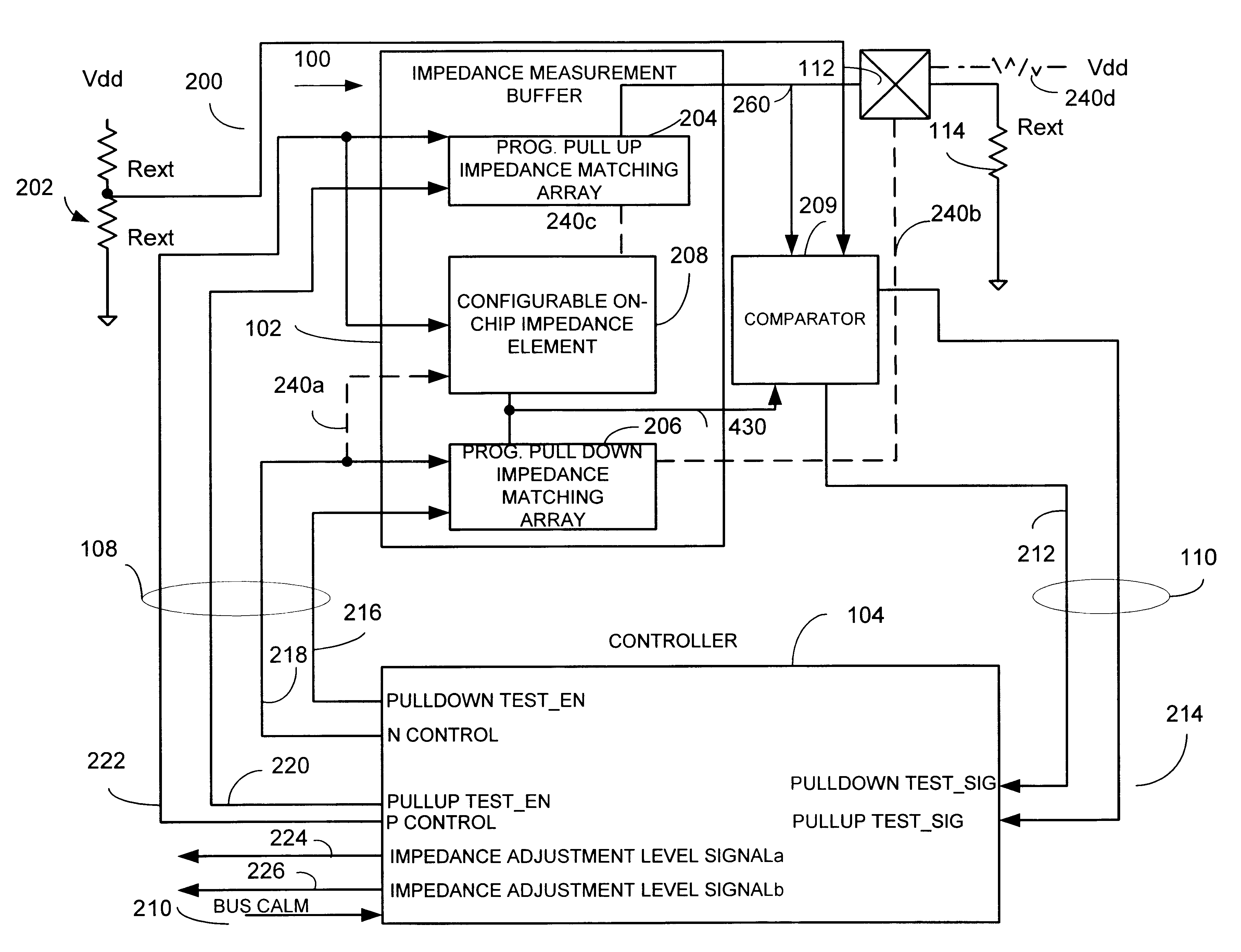
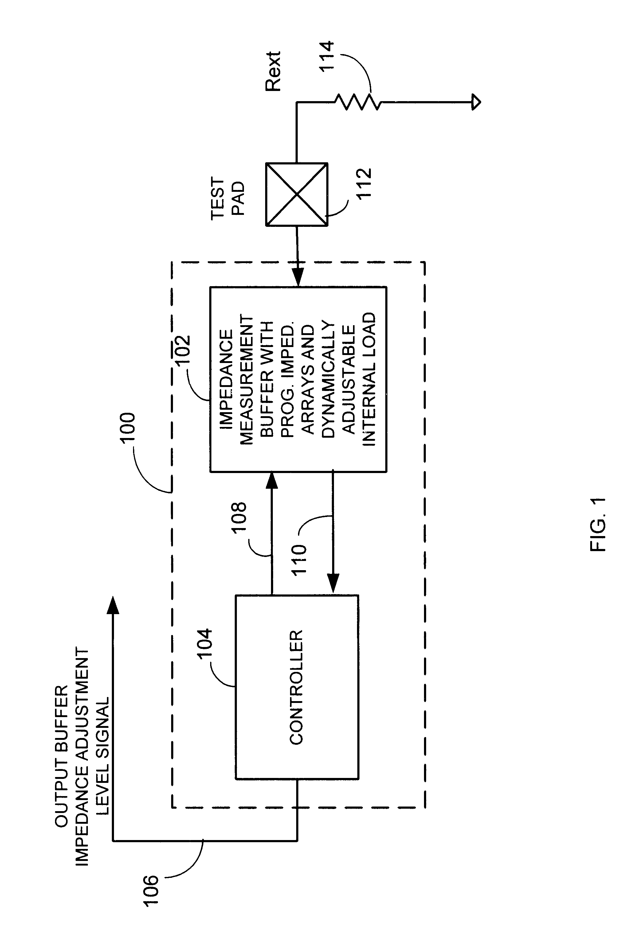
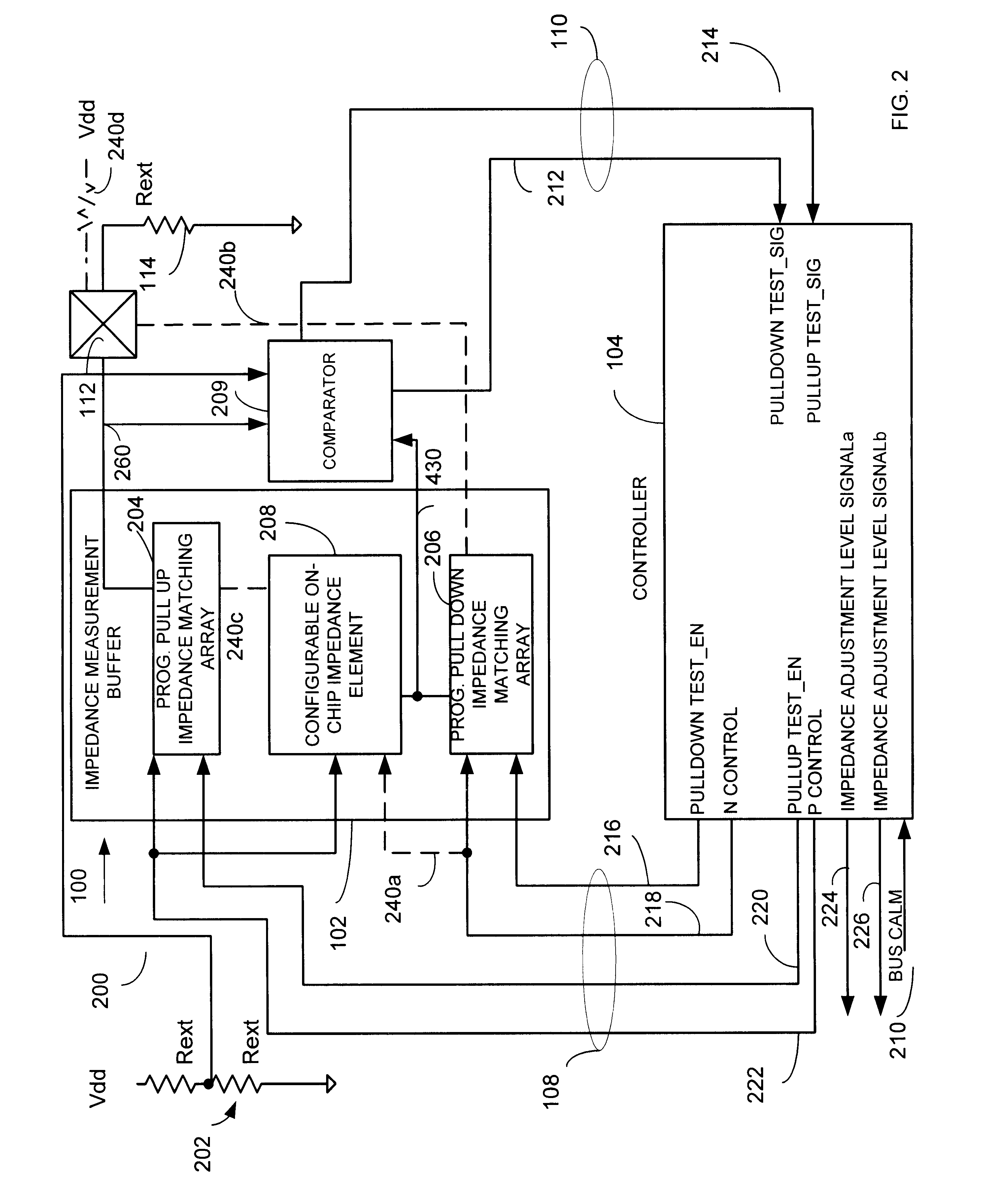
Briefly, an impedance compensation circuit and method for an input / output buffer provides dynamic impedance compensation by using programmable impedance arrays and a dynamically adjustable on-chip load. Accordingly, among other advantages, only a single off-chip calibration resistor is used, and only a single test pad is necessary.

In one embodiment, the impedance compensation circuit includes an on-chip programmable pull up impedance matching array, such as a plurality of parallel coupled PMOS transistor fingers, an on-chip programmable pull down impedance matching array, such as a plurality of NMOS parallel coupled transistor fingers, and a configurable on-chip impedance element, such as a plurality of parallel coupled PMOS transistors. The configurable on-chip impedance measurement array is operatively coupled to both the on-chip programmable pull up impedance matching array, and to the on-chip programmable pull down impedance matching array.

In one embodiment, a controller control...


PUM


Abstract

An impedance compensation circuit and method for an input / output buffer provides dynamic impedance compensation by using programmable impedance arrays and a dynamically adjustable on-chip load. Accordingly, among other advantages, only a single off-chip or external calibrated impedance resistor is used and only a single test pad is necessary.

Description

The invention relates generally to impedance matching networks and more particularly to programmable on-chip impedance matching networks.Background Of The Invention Input / output buffers are used in many integrated circuit applications. Conventional I / O buffers include, for example, push / pull buffer configurations that include, for example, an output driver pull up circuit and an output driver pull down circuit. I / O buffers are often connected to external or off chip pads on printed circuit boards or other integrated circuits. The I / O buffers are connected to other circuits through transmission lines, such as printed circuit boards traces or any other suitable transmission line. As is known in the art, transmission line signal distortions can result from impedance mismatches between the output buffer circuitry, and the transmission line impedance. These signal distortions can vary due to fabrication process variations, temperature variations, and other variations. Accordingly, I / O bu...

Claims


Application Information

Patent Timeline
Patent Type & Authority Patents(United States)
IPC IPC(8): H03K19/00
CPCH03K19/0005
Inventor ROSEFIELD, PETER L.DRAPKIN, OLEGTEMKINE, GRIGORICARUK, GORDON F.THAMBIMUTHU, ROCHESAHDRA, KULDIPBALATSOS, ARIS
Owner ATI TECH INC
Why Eureka
Try Eureka