Silicon interposer and multi-chip-module (MCM) with through substrate vias

a silicon interposer and substrate technology, applied in the direction of semiconductor devices, semiconductor/solid-state device details, electrical apparatus, etc., can solve the problems of electrical opening in the package, cracks, and stress in the solder bumps

Inactive Publication Date: 2003-05-13
INTEL CORP
View PDF14 Cites 259 Cited by
  • Summary
  • Abstract
  • Description
  • Claims
  • Application Information

AI Technical Summary

Problems solved by technology

The mismatch of thermal expansion coefficients may create stresses in the solder bumps when the package is thermally cycled.
The stresses may create cracks, and electrical opens in the package.
Even with the epoxy underfill it has been found that the substrate may delaminate and crack when the package thermally cycled.
Heat slugs and heat spreaders may not be adequate to effectively remove all of the heat from a high powered integrated circuit such as a microprocessor.
Organic substrates of the prior art have a relatively low coefficient of thermal conductivity.

Method used


Image

  • Silicon interposer and multi-chip-module (MCM) with through substrate vias
  • Silicon interposer and multi-chip-module (MCM) with through substrate vias
  • Silicon interposer and multi-chip-module (MCM) with through substrate vias

Examples


Embodiment Construction

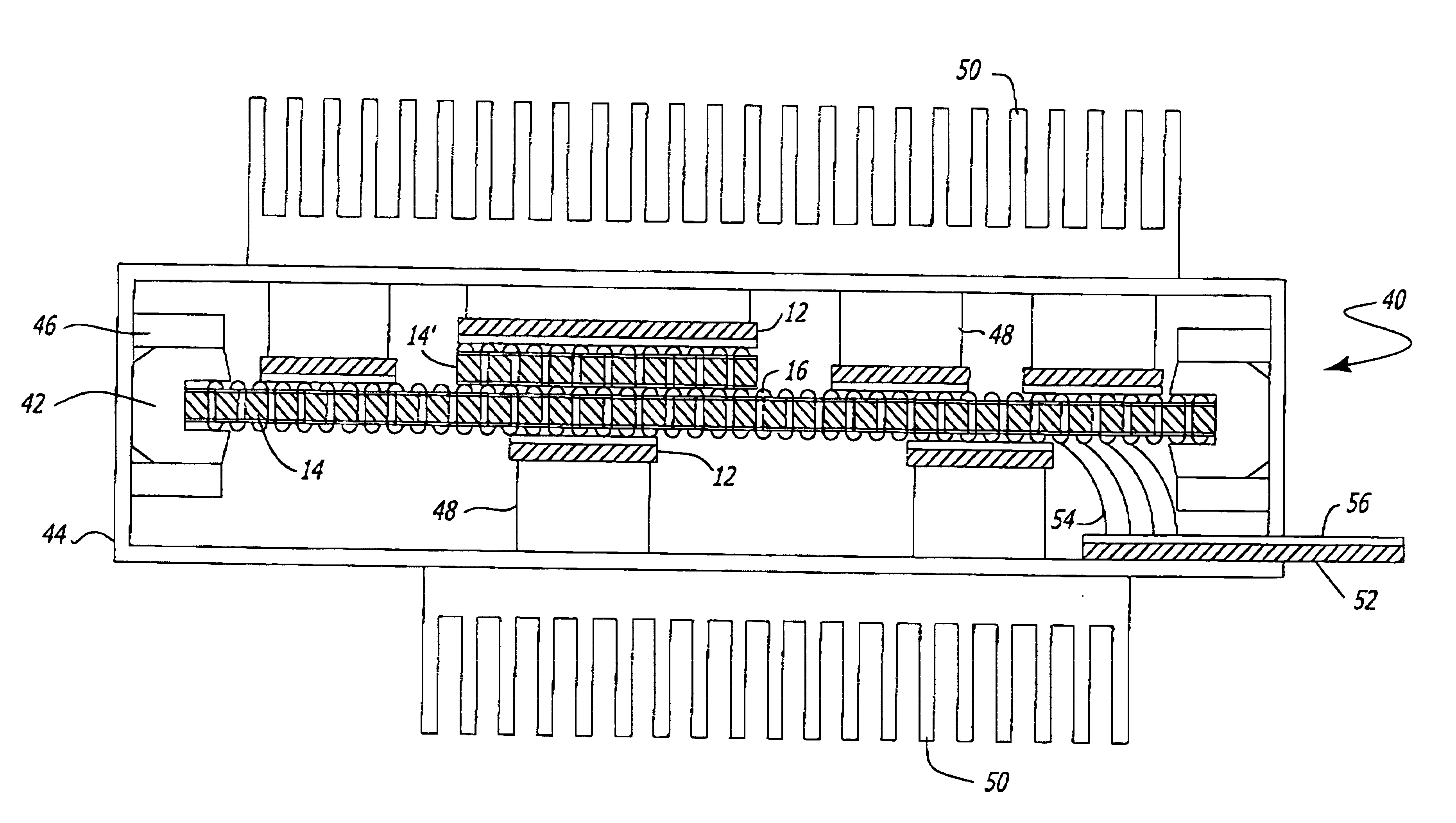
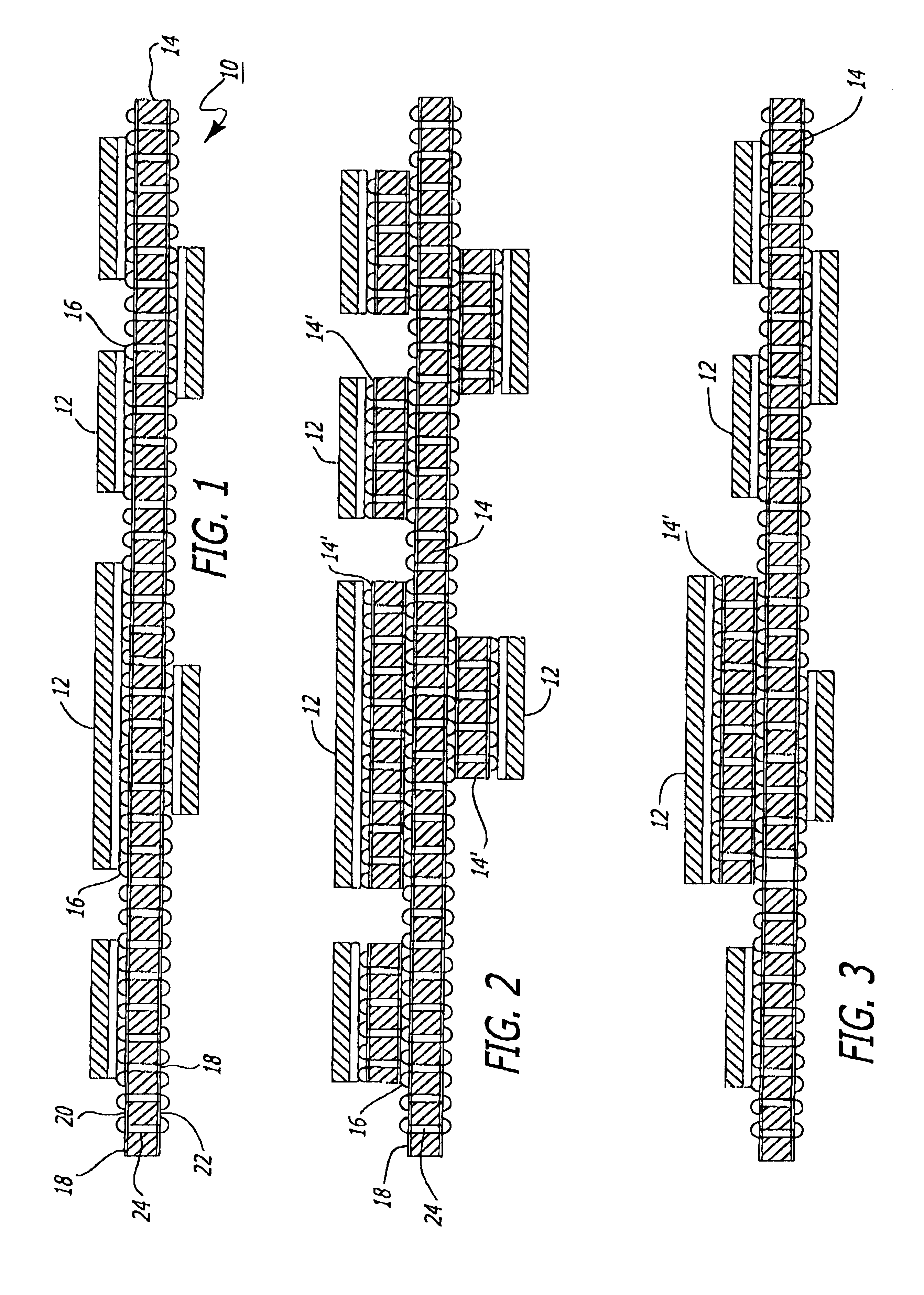
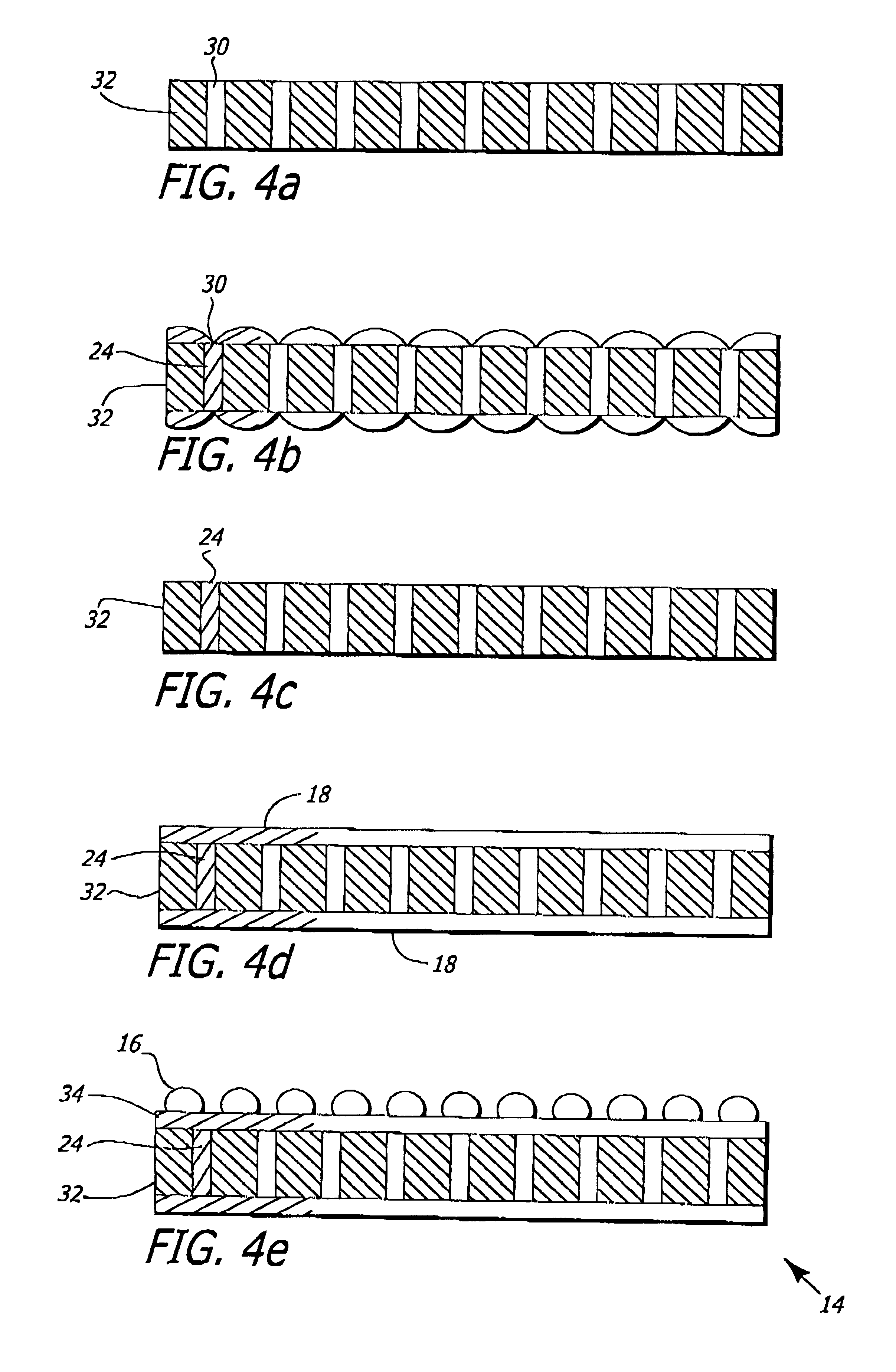
Referring to the drawings more particularly by reference numbers, FIG. 1 shows an embodiment of an electronic package 10 of the present invention. The package 10 may include a plurality of integrated circuits 12 that are connected to a silicon substrate 14. The integrated circuits 12 may be connected to the substrate 14 by solder bumps 16 with a process commonly referred to as controlled collapsed chip connection (C4).

The substrate 14 is constructed from silicon which has a coefficient of thermal expansion that matches the coefficient of thermal expansion of the integrated circuits. When the package 10 is thermally cycled the integrated circuit 12 and the substrate 14 expand at approximately the same rate. The matched expansion reduces the stresses on the solder bumps 16 over prior art packages which incorporate substrates that do not have a coefficient of thermal expansion that matches. Additionally, silicon has a higher coefficient of thermal conductivity than organic substrates o...


PUM


Abstract

An integrated circuit package which includes an integrated circuit that is connected to a silicon substrate. The silicon substrate may have a via. The package may further include a solder bump that is attached to both the integrated circuit and the silicon subtstrate. The silicon substrate has a coefficient of thermal expansion that matches the coefficient of thermal expansion of the integrated circuit.

Description

BACKGROUND OF THE INVENTION1. Field of the InventionThe present invention relates to an integrated circuit package.2. Background InformationIntegrated circuits are typically assembled into packages that are soldered to a printed circuit board. Each integrated circuit may be connected to a substrate of the package with a number of solder bumps in a process commonly referred to as controlled collapsed chip connection (C4).During operation, the integrated circuit generates heat which raises the temperature of the package. Additionally, the package temperature may be increased during assembly of the package. The increase in package temperature will cause the integrated circuit and the substrate to expand. The substrate is typically constructed as a composite of metal and organic material which have a different coefficient of thermal expansion than the silicon material of the integrated circuit. The mismatch of thermal expansion coefficients may create stresses in the solder bumps when t...

Claims


Application Information

Patent Timeline
Patent Type & Authority Patents(United States)
IPC IPC(8): H01L23/48H01L25/065H01L23/498
CPCH01L23/49827H01L25/0652H01L2224/16H01L2924/3011
Inventor MA, QINGFUJIMOTO, HARRY
Owner INTEL CORP
Why Eureka
Try Eureka