Integrated circuit packaging system with stackable package and method of manufacture thereof

a technology of integrated circuit and stackable packaging, which is applied in the direction of semiconductor devices, semiconductor/solid-state device details, electrical apparatus, etc., can solve the problems of direct impact on the availability, reliability, yield and cost of products, and the solution to these problems has long eluded those skilled in the ar

Active Publication Date: 2011-06-02
STATS CHIPPAC LTD
View PDF8 Cites 10 Cited by
  • Summary
  • Abstract
  • Description
  • Claims
  • Application Information

AI Technical Summary

Problems solved by technology

Each of the integrated circuit packages within the cell phone can contain large amounts of complex circuitry.
Furthermore, the ways the circuitry and electrical connections are implemented have a direct impact on the availability, reli...

Method used


Image

  • Integrated circuit packaging system with stackable package and method of manufacture thereof
  • Integrated circuit packaging system with stackable package and method of manufacture thereof
  • Integrated circuit packaging system with stackable package and method of manufacture thereof

Examples


first embodiment

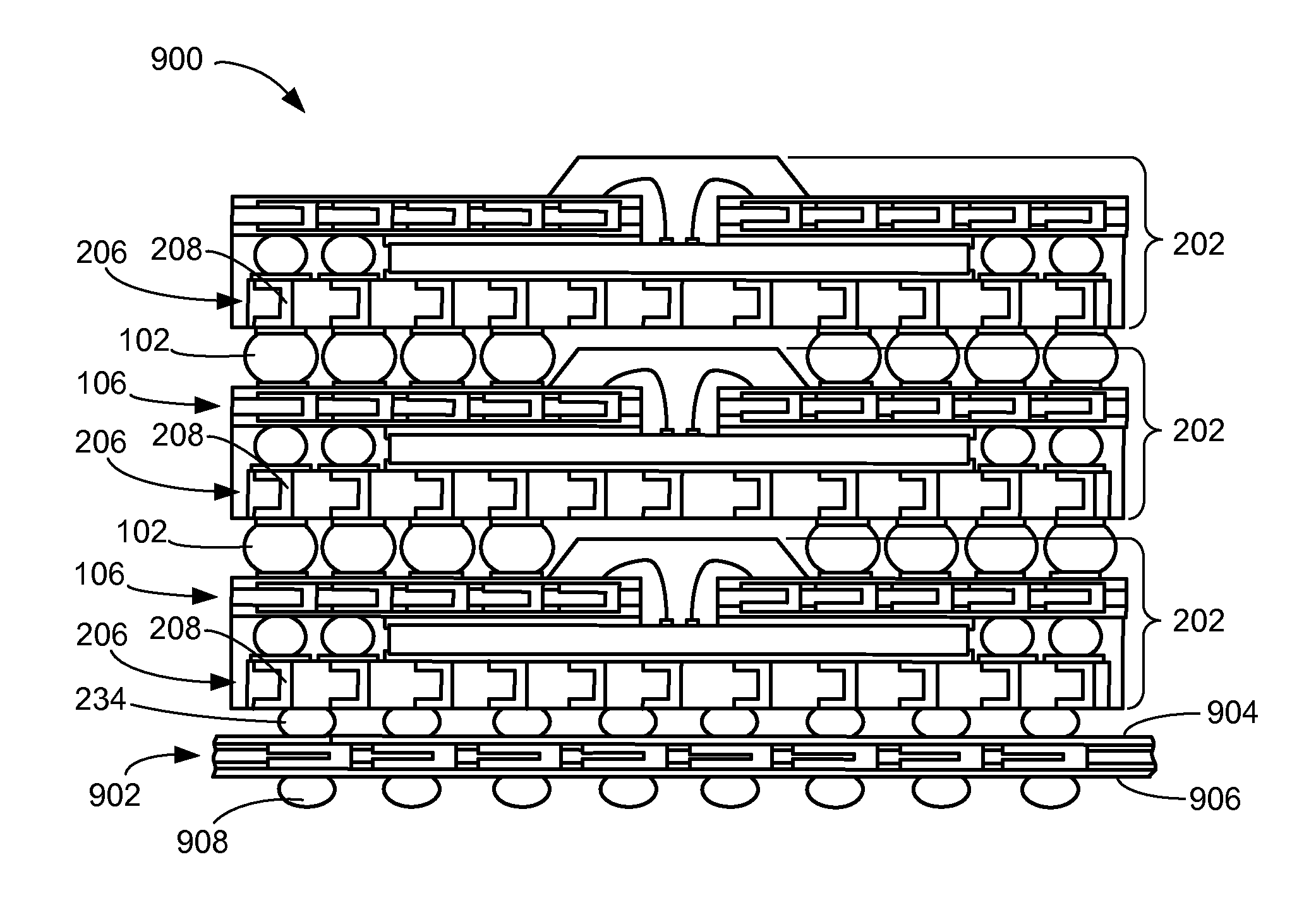
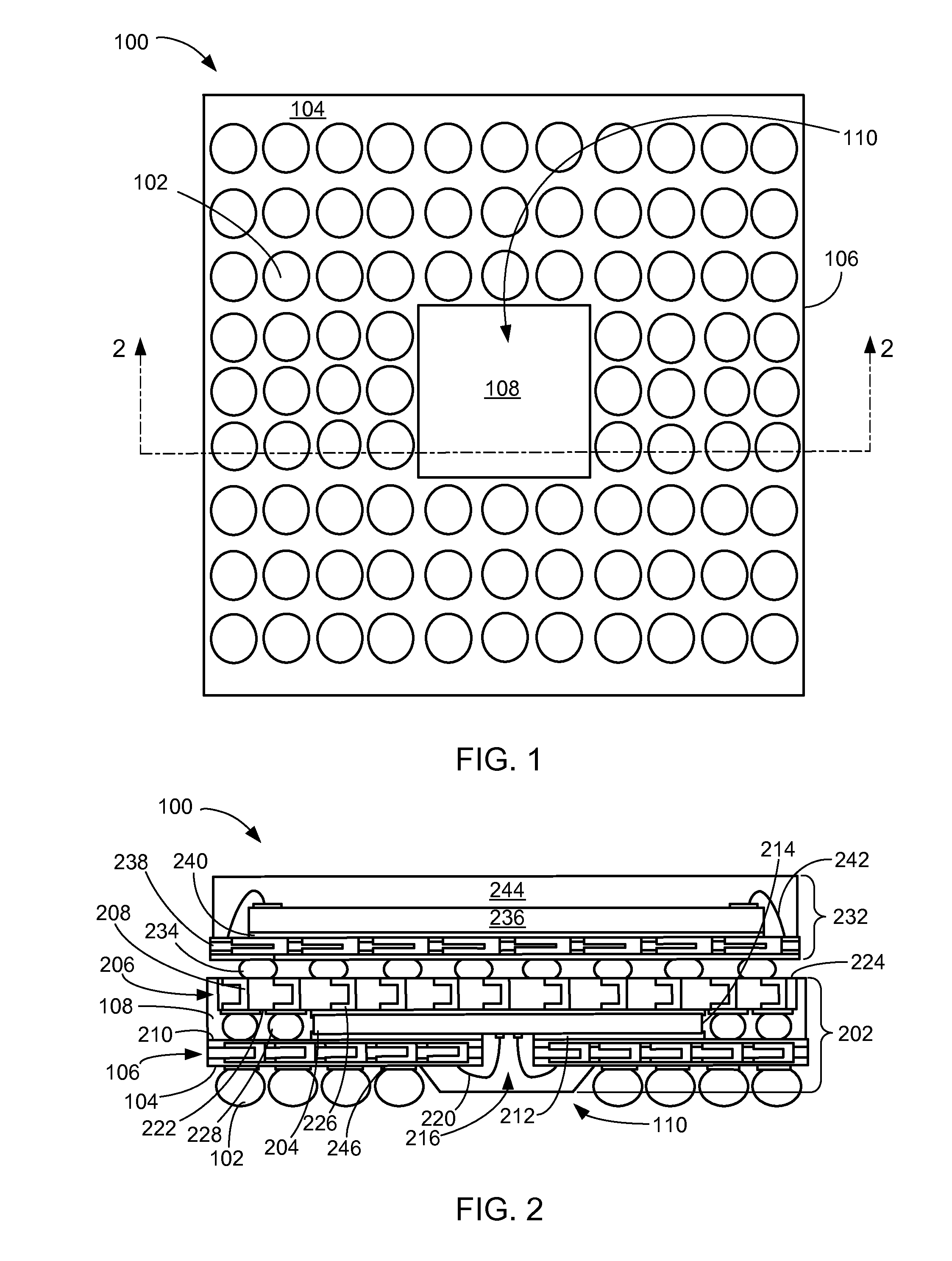
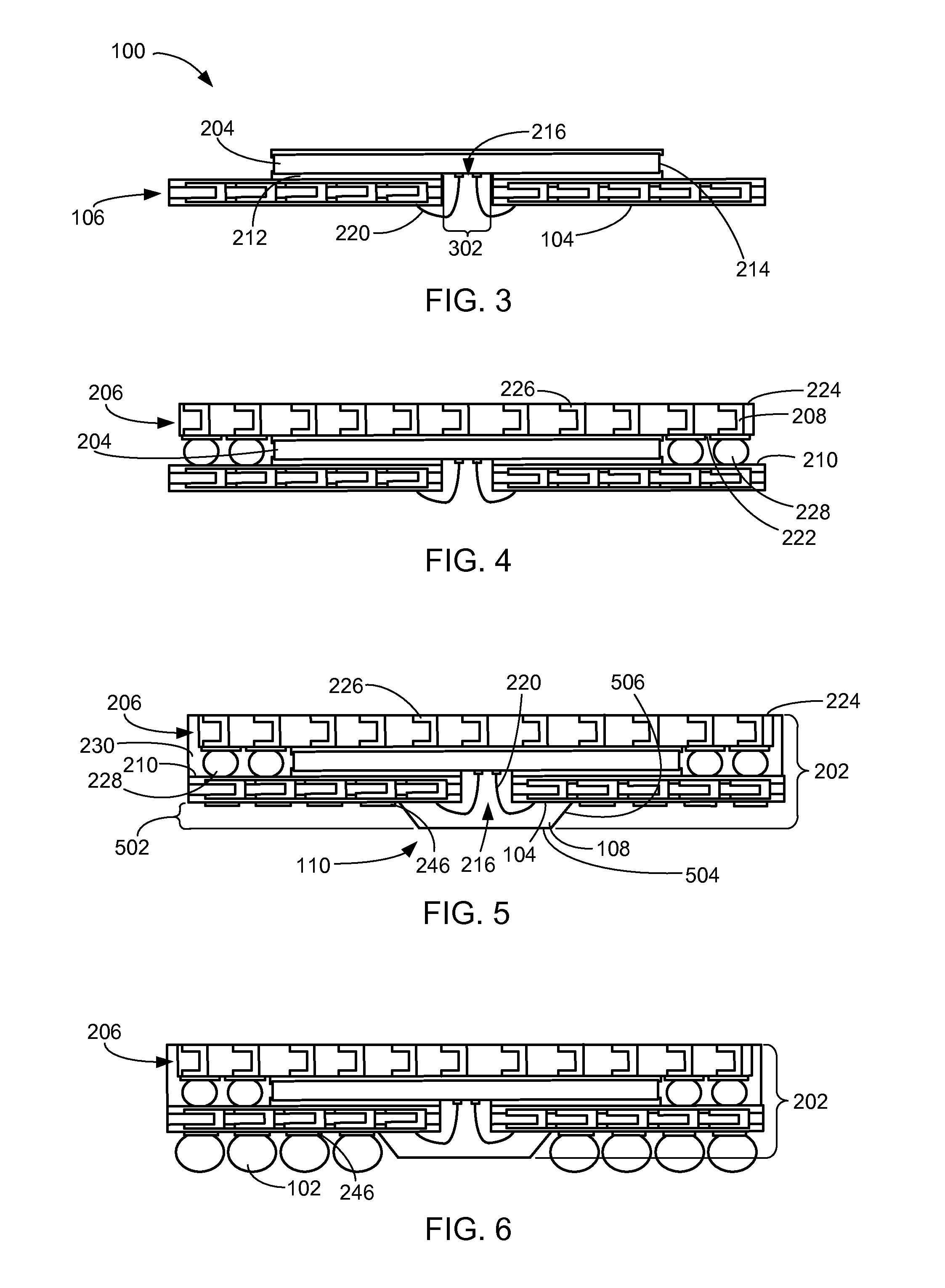
[0030]Referring now to FIG. 1, therein is shown a bottom view of an integrated circuit packaging system 100 in the present invention. Package connectors 102, such as conductive balls, bumps, or pads are shown connecting to an outward base side 104 of a package base 106, such as a board, a substrate, or a circuit board.

[0031]For illustrative purposes, the package connectors 102 are shown having a circular shape and formed in rows parallel to or perpendicular to sides of the package base 106 although the package connectors 102 can have any shape, size, orientation, or configuration. For example, the package connectors 102 can have a square shape or have a random distribution across the outward base side 104.

[0032]The package connectors 102 are shown surrounding an encapsulant 108, such as an epoxy, an epoxy blend, a silicone material, a polyimide, or a combination thereof, formed as a protrusion 110 having a shape of a rectangle. The protrusion 110 can have any size, shape, or locatio...

second embodiment

[0059]Referring now to FIG. 7, therein is shown a cross-sectional view of an integrated circuit packaging system 700 in the present invention. The integrated circuit packaging system 700 can preferably include a stack package 702 having a device 704, similar to the device 204 of FIG. 2, the silicon interposer 206, and a package base 706 oriented in a manner similar to the device 204 of FIG. 2 and the package base 106 of FIG. 2.

[0060]The package base 706, similar to the package base 106, can include an outward base side 708 and an inward base side 710 opposite the outward base side 708. An adhesive layer 712, similar to the adhesive layer 212 of FIG. 2, can be applied on to ends 714 and sides of the device 704 in a manner similar to the adhesive layer 212 of FIG. 2, the ends 214 of FIG. 2, and the active side and the side opposite the active side of the device 204. The device 704 can be mounted between the silicon interposer 206 and the package base 706 using the adhesive layer.

[0061...

third embodiment

[0070]Referring now to FIG. 8, therein is shown a cross-sectional view of an integrated circuit packaging system 800 in the present invention. The integrated circuit packaging system 800 can preferably include a stack package 802, such as a stack, a board on die, or a board on module package, having a device 804, a silicon interposer 806 with through silicon vias 808, and a package base 810.

[0071]The device 804, such as a chip, a module, or an integrated circuit package, can preferably have planar dimensions smaller than planar dimensions of the silicon interposer 806. The package base 810, such as a board, a substrate, or a circuit board, can preferably have planar dimensions smaller than the planar dimensions of the device 804.

[0072]The stack package 802 can include an active side of the device 804 mounted over an inward base side 812 of the package base 810 opposite the outward base side 814 using an adhesive layer 816. Conductive materials within the package base 810, on the out...


PUM


Abstract

A method of manufacture of an integrated circuit packaging system includes: providing a package base having an inward base side and an outward base side; mounting a device over the inward base side and connected to the outward base side; connecting a silicon interposer having a through silicon via to the device and having an external side facing away from the device; and applying an encapsulant around the device, over the package base, and over the silicon interposer with the external side substantially exposed, the encapsulant having a protrusion over the outward base side.

Description

TECHNICAL FIELD[0001]The present invention relates generally to an integrated circuit packaging system, and more particularly to a package on package system.BACKGROUND ART[0002]A tremendous market growth for high density and high output / input integrated circuit packages has resulted in a trend for electronic products that are lightweight, smaller in size, multi-functional, and with higher speeds. Electronic products such as cell phone base products, global positioning systems (GPS), satellites, communication equipment, consumer products, and a vast line of other similar products are in ever increasing global demand.[0003]Products must compete in world markets and attract many consumers or buyers in order to be successful. It is very important for products to continue to improve in features, performance, and reliability while reducing product costs, product size, and equally important to be available quickly for purchase by the consumers or buyers.[0004]Therefore, there is an importa...

Claims


Application Information

Patent Timeline
IPC IPC(8): H01L23/52H01L21/98
CPCH01L23/3128H01L23/49816H01L2225/1058H01L2225/1041H01L2225/1023H01L24/48H01L2924/15331H01L2924/15311H01L2924/14H01L2224/73265H01L2224/73215H01L2224/4824H01L2224/48227H01L2224/48091H01L2224/32225H01L25/105H01L23/49833H01L23/49827H01L2924/00014H01L2924/00012H01L24/73H01L2224/45099H01L2224/45015H01L2924/207
Inventor YANG, DEOKKYUNGCHOI, DAESIK
Owner STATS CHIPPAC LTD
Why Eureka
Try Eureka