Wafer scale packaging platform for transceivers

a packaging platform and optical transceiver technology, applied in the field of optical transceivers with a wavelength scale, can solve the problems of time-consuming and expensive, and achieve the effect of reducing the cost of unit-by-unit active optical alignmen

Inactive Publication Date: 2014-08-12
CISCO TECH INC
View PDF49 Cites 10 Cited by
  • Summary
  • Abstract
  • Description
  • Claims
  • Application Information

AI Technical Summary

Benefits of technology

[0008]In further accordance with the present invention, the utilization of a silicon interposer allows for various through-silicon vias to be formed and used to provide electrical connections between components placed on the interposer and underlying electrical components. Electronic integrated circuits such as laser drivers, micro-controllers and transimpedance amplifiers are accurately placed on the silicon interposer using photolithographically-aided features formed on the interposer. Wafer scale wirebonding techniques are used to create the necessary electrical connections between the individual elements. Optical components such as lasers, isolators, lenses (individual and arrays), photodiodes and the like are placed within lithographically-defined openings on the interposer, where the ability accurately and precisely define the location and size of openings using conventional CMOS fabrication techniques allows for passive optical alignment processes to be used where appropriate.

Problems solved by technology

In most cases, these transceiver modules are built as individual units and, as a result, the need to perform active optical alignment on a unit-by-unit basis becomes expensive and time-consuming.
As the demand for optical transceiver modules continues to increase, the individual unit assembly approach becomes problematic and, therefore, a need remains for a different approach to optical transceiver assembly that can improve the efficiency of the construction process while preserving the integrity of module, including the required precise optical alignment between elements.

Method used


Image

  • Wafer scale packaging platform for transceivers
  • Wafer scale packaging platform for transceivers
  • Wafer scale packaging platform for transceivers

Examples


Embodiment Construction

[0033]In the following description, for purposes of explanation and not limitation, specific details are set forth in order to provide a thorough understanding of the present invention. However, it will be apparent to one skilled in the art that the present invention may be practiced in other embodiments that depart from these specific details. In other instances, detailed descriptions of well-known devices and methods are omitted so as not to obscure the description of the present invention with unnecessary details.

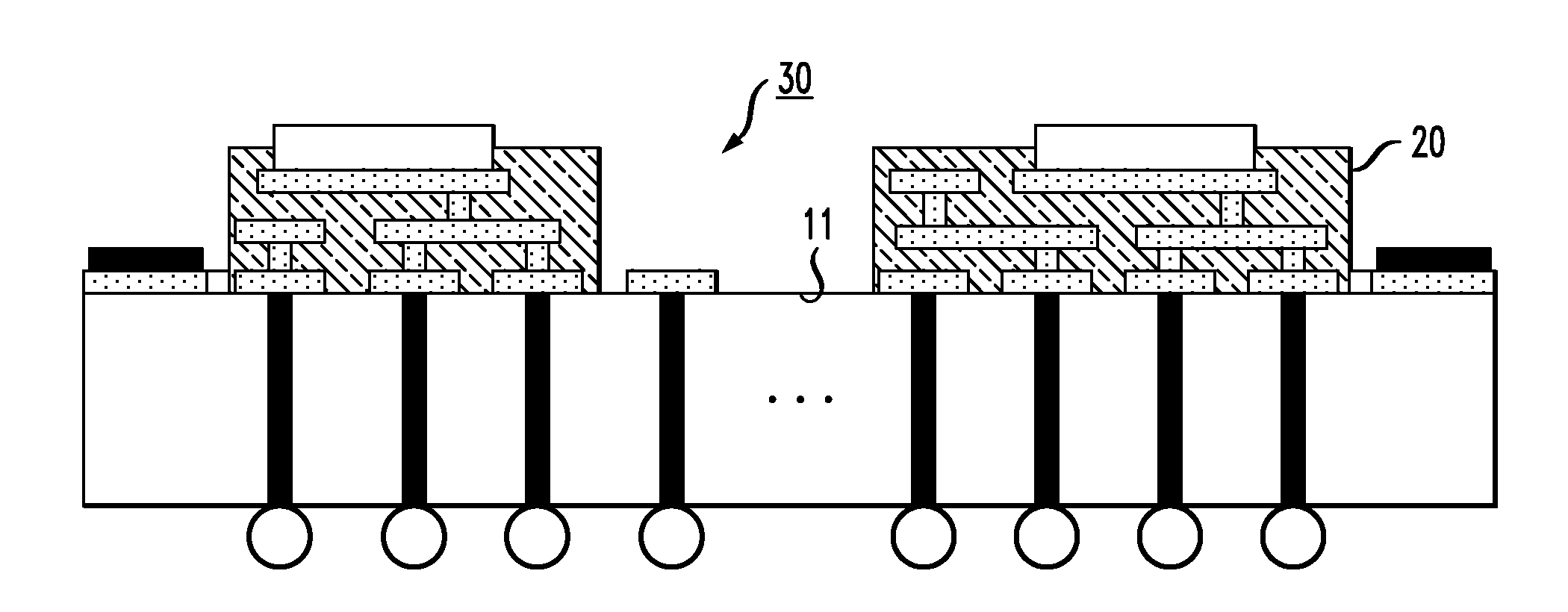
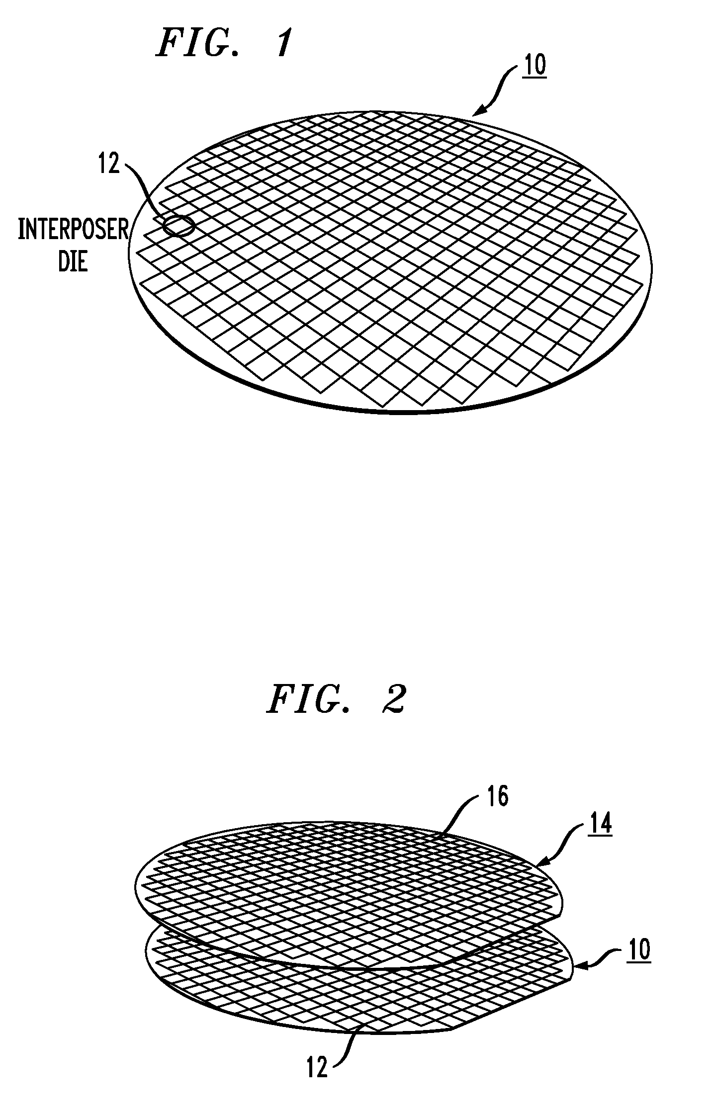
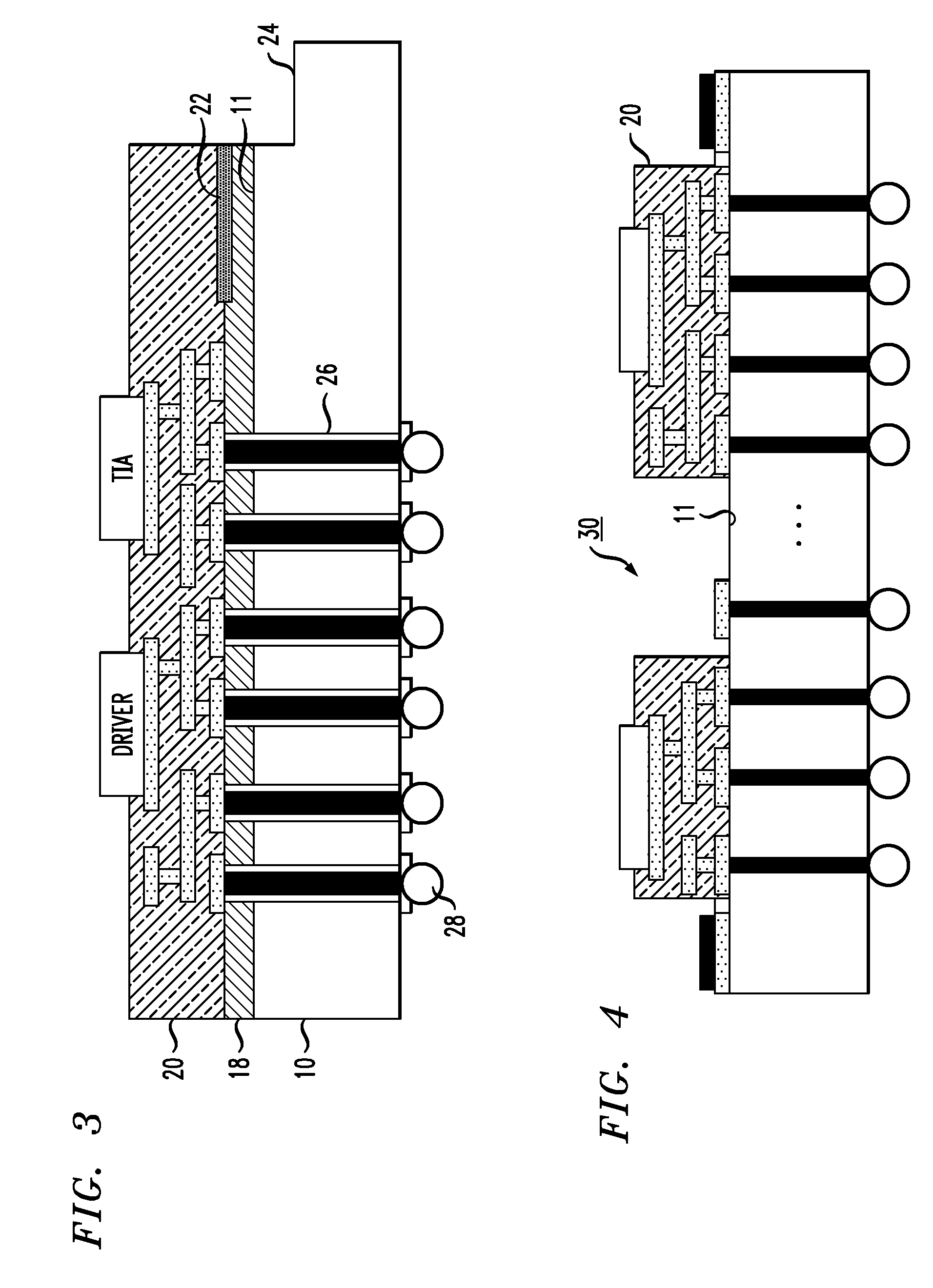
[0034]As mentioned above, a significant improvement in fabrication efficiency, without sacrificing the integrity of the necessary precise optical alignments between various individual elements, is provided in accordance with the present invention by utilizing a wafer scale assembly technique, employing a silicon wafer as a carrier substrate (also referred to hereinafter as an interposer) upon which the individual components (including electronic integrated circuits, acti...


PUM


Abstract

A wafer scale implementation of an opto-electronic transceiver assembly process utilizes a silicon wafer as an optical reference plane and platform upon which all necessary optical and electronic components are simultaneously assembled for a plurality of separate transceiver modules. In particular, a silicon wafer is utilized as a “platform” (interposer) upon which all of the components for a multiple number of transceiver modules are mounted or integrated, with the top surface of the silicon interposer used as a reference plane for defining the optical signal path between separate optical components. Indeed, by using a single silicon wafer as the platform for a large number of separate transceiver modules, one is able to use a wafer scale assembly process, as well as optical alignment and testing of these modules.

Description

CROSS-REFERENCE TO RELATED APPLICATIONS[0001]This application claims the benefit of the following U.S. Provisional Applications: Ser. No. 61 / 482,705, filed May 5, 2011; Ser. No. 61 / 509,290, filed Jul. 19, 2011; Ser. No. 61 / 526,821, filed Aug. 24, 2011; Ser. No. 61 / 543,240, filed Oct. 4, 2011; and Ser. No. 61 / 560,378, filed Nov. 16, 2011, all of which are incorporated by reference herein.TECHNICAL FIELD[0002]The present invention relates to a wafer scale implementation of opto-electronic transceivers and, more particularly, to the utilization of a silicon wafer as an optical reference plane and platform upon which all necessary optical and electronic components are assembled for a multiple number of transceivers in a wafer scale process.BACKGROUND OF THE INVENTION[0003]In optical communication networks, transceivers are used to transmit and receive optical signals over optical fibers or other types of optical waveguides. On the transmit side of the transceiver, a laser diode and asso...

Claims


Application Information

Patent Timeline
Patent Type & Authority Patents(United States)
IPC IPC(8): H01L31/0232H01L29/40H01L23/12H01L23/053
CPCH01L25/167G02B6/4249H01L25/50G02B6/426G02B6/423G02B6/4244G02B6/4245G02B6/4257H01L2224/16225H01L2224/48091H01L2224/48227H01L2924/00014
Inventor SHASTRI, KALPENDUPATEL, VIPULKUMARWEBSTER, MARKGOTHOSKAR, PRAKASHKACHRU, RAVINDERPATHAK, SOHAMYELAMARTY, RAO V.DAUGHERTY, THOMASDAMA, BIPINPATEL, KAUSHIKDESAI, KISHOR
Owner CISCO TECH INC
Why Eureka
Try Eureka