Large sized silicon interposers overcoming the reticle area limitations

An interposer and intermediary technology, applied in the field of interconnection, can solve the problems of increasing cost, reducing output, and not being easy to manufacture.

Active Publication Date: 2015-02-11
HUAWEI TECH CO LTD
View PDF4 Cites 9 Cited by
  • Summary
  • Abstract
  • Description
  • Claims
  • Application Information

AI Technical Summary

Problems solved by technology

However, interposer substrates of this size are either not easy to fabricate or require dedicated photolithography processes, which will significantly increase cost (and possibly reduce yield)

Method used


Image

  • Large sized silicon interposers overcoming the reticle area limitations
  • Large sized silicon interposers overcoming the reticle area limitations
  • Large sized silicon interposers overcoming the reticle area limitations

Examples


Embodiment Construction

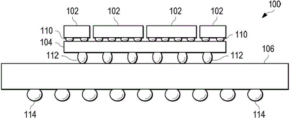
[0016] In general, the present invention describes and teaches the design and construction of a new 2.5D IC package assembly that enables The package size is larger overall. As shown in FIG. 1 , existing technology is limited by dies mounted on a silicon interposer whose total area is less than the area of ​​the silicon interposer. Therefore, if the die is large, its composability with other dies to 2.5D IC package components is limited. By aligning only portions of multiple dies over the "active area," larger dies and / or greater numbers of dies can be combined and assembled into a single package.

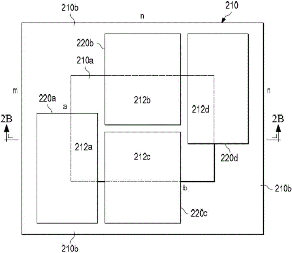
[0017] For the purposes of this patent document, the term "active area" in a silicon interposer refers to areas where TSVs and other interconnecting conductors (such as power, ground, and other area formed for the photomask).

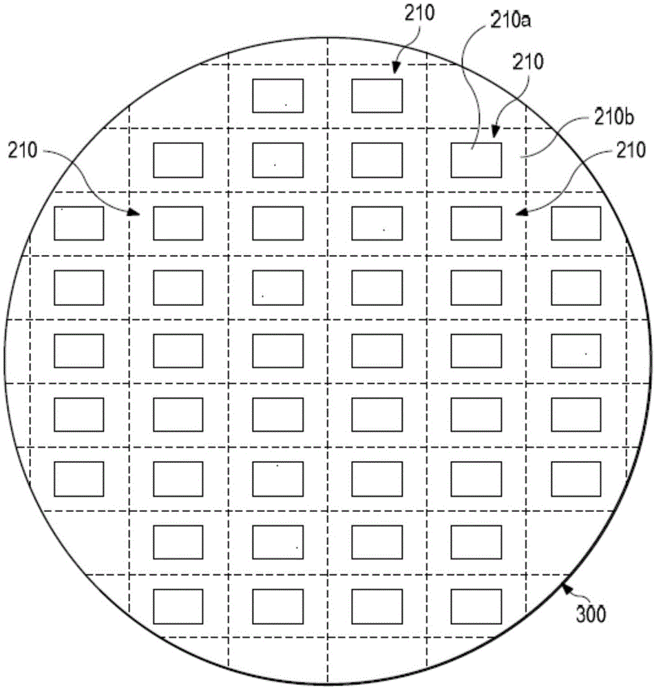
[0018] Figure 2A and Figure 2B Top and cross-sectional views, respectively, of an example multi-die integrated circuit package 200 according to the pr...


PUM


Abstract

A multi-die integrated circuit assembly includes an interposer substrate larger than the typical reticle size used in fabricating the "active area" in which the through-silicon vias (TSVs) and interconnect conductors are formed in the interposer. At the same time, each of the dies has its external power / ground and I / O signal line connections concentrated into a smaller area of the die. The dies are disposed or mounted on the interposer such that these smaller areas (with the power / ground / IO connections) overlap with the active area of the interposer. In this configuration, a plurality of dies having a combined area substantially greater than the active area of the interposer can be mounted on the interposer (and take advantage of the active area for interconnections).

Description

[0001] Related Applications Cross Application [0002] This application claims prior application priority to U.S. Patent Application No. 13 / 551,466, filed July 17, 2012, entitled "Large Silicon Interposer Overcoming Reticle Area Limitations," which is incorporated in its entirety incorporated into this text technical field [0003] The present invention relates to interconnection technology, and more particularly to methods and silicon interposer structures for use in multi-die integrated circuit packaging. Background technique [0004] A 2D integrated circuit package (2D IC package) is a single package constructed by mounting multiple semiconductor wafers / chips / chips and interconnecting them horizontally to function as a single device or system. A 3D integrated circuit package (3D IC package) or 3-dimensional stacked integrated circuit package (3DS IC package) is a single integrated package constructed by vertically stacking individual semiconductor wafers / chips / chips and ...

Claims


Application Information

Patent Timeline
Patent Type & Authority Applications(China)
IPC IPC(8): H01L23/48
CPCH01L2924/15192H01L25/0655H01L2924/15311H01L2224/17517H01L23/5385H01L23/5383H01L2224/16225H01L23/5384H01L23/147H01L2224/16235H01L24/17H01L2224/16227H01L2924/157
Inventor 宋浩宇曹玮牛瑞安瓦尔·穆罕默德
Owner HUAWEI TECH CO LTD
Why Eureka
Try Eureka